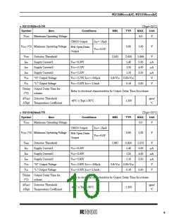
R3130N×××A/C, R3131N×××A/C
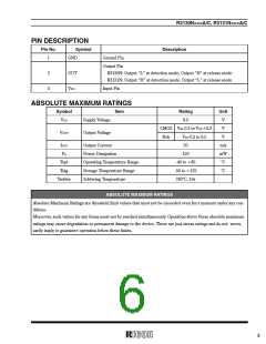
PIN DESCRIPTION
Pin No.
Symbol
Description
1
GND
Ground Pin
Output Pin
2
3
OUT
VDD
R3130N: Output “L” at detection mode, Output “H” at release mode
R3131N: Output “H” at detection mode, Output “L” at release mode
Input Pin
ABSOLUTE MAXIMUM RATINGS
Symbol
Item
Rating
6.5
Unit
V
VDD
Supply Voltage
Output Voltage
Output Current
CMOS VSS-0.3 to VDD+0.3
V
VOUT
Nch
VSS-0.3 to 6.5
V
IOUT
PD
20
mA
mW
°C
Power Dissipation
150
Topt
Tstg
Operating Temperature Range
Storage Temperature Range
Soldering Temperature
-40 to +85
-55 to +125
260°C, 10s
°C
Tsolder
ABSOLUTE MAXIMUM RATINGS
Absolute Maximum Ratings are threshold limit values that must not be exceeded even for a moment under any con-
ditions.
Moreover, such values for any items must not be reached simultaneously. Operation above these absolute maximum
ratings may cause degradation or permanent damage to the device. These are just stress ratings and do not neces-
sarily imply to guarantee operation below these limits.
5

 RICOH [ RICOH ELECTRONICS DEVICES DIVISION ]