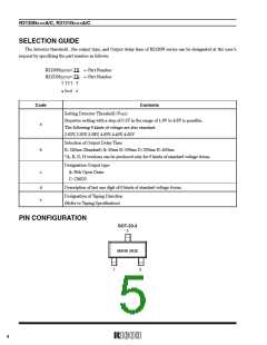
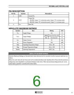
R3130N×××A/C, R3131N×××A/C
TIMING CHART
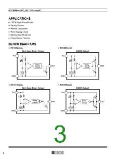
Detector
Detector
Threshold
Threshold
V
DET
V
DET
Supply
Voltage
Supply
Voltage
(VDD)
Minimum Operating
Voltage
Minimum Operating
Voltage
(VDD
)
V
SS
V
SS
Output Voltage
Output Voltage
V
SS
V
SS
Tdelay
Tdelay
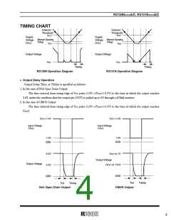
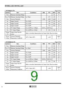
R3130N Operation Diagram
R3131N Operation Diagram
• Output Delay Operation
Output Delay Time, or Tdelay is specified as follows:
1. In the case of Nch Open Drain Output:
The time interval from rising edge of VDD pulse (1.0V→(VDET)+0.1V) to the time at which the output reaches
2.5V under the condition that the output pin (OUT) is pulled up to 5V through a 470kΩ resistor.
2. In the case of CMOS Output
The time interval from rising edge of VDD pulse (1.0V→(VDET)+0.1V) to the time at which the output reaches
VDD/2.
V
DET+1.0V
VDET+1.0V
Input Voltage
(VDD
Input Voltage
(VDD
)
)
1.0V
GND
1.0V
GND
V
DET+0.1V
5.0V
2.5V
GND
Output Voltage
(VDET+0.1V)/2
Output Voltage
GND
Trst
Tdelay
Trst
Tdelay
Nch Open Drain Output
CMOS Output
3

 RICOH [ RICOH ELECTRONICS DEVICES DIVISION ]