RT9183
Parameter
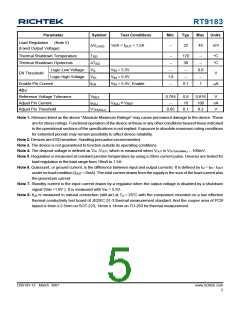
Load Regulation (Note 5)
Symbol
Test Conditions
1mA < I < 1.5A
Min
Typ
Max
Units
ΔV
--
22
45
mV
LOAD
OUT
(Fixed Output Voltage)
Thermal Shutdown Temperature
Thermal Shutdown Hysteresis
T
--
--
170
30
--
--
--
°C
°C
SD
ΔT
SD
Logic-Low Voltage
EN Threshold
V
V
I
V
IN
V
IN
V
IN
= 5.5V
--
0.6
--
IL
IH
V
Logic-High Voltage
= 5.5V
= 5.5V, Enable
1.8
--
--
Enable Pin Current
ADJ
0.1
1
μA
EN
Reference Voltage Tolerance
Adjust Pin Current
Adjust Pin Threshold
V
0.784
--
0.8
10
0.816
100
V
nA
V
REF
I
V
ADJ = V
ADJ
REF
V
0.05
0.1
0.2
TH(ADJ)
Note 1. Stresses listed as the above "Absolute Maximum Ratings" may cause permanent damage to the device. These
are for stress ratings. Functional operation of the device at these or any other conditions beyond those indicated
in the operational sections of the specifications is not implied. Exposure to absolute maximum rating conditions
for extended periods may remain possibility to affect device reliability.
Note 2. Devices are ESDsensitive. Handling precaution recommended.
Note 3. The device is not guaranteed to function outside its operating conditions.
Note 4. The dropout voltage is defined as VIN -VOUT, which is measured when VOUT is VOUT(NORMAL) − 100mV.
Note 5. Regulation is measured at constant junction temperature by using a 20ms current pulse. Devices are tested for
load regulation in the load range from 10mA to 1.5A.
Note 6. Quiescent, or ground current, is the difference between input and output currents. It is defined by IQ = IIN - IOUT
under no load condition (IOUT = 0mA). The total current drawn from the supply is the sum of the load current plus
the ground pin current.
Note 7. Standby current is the input current drawn by a regulator when the output voltage is disabled by a shutdown
signal (VEN >1.8V ). It is measured with VIN = 5.5V.
Note 8. θJA is measured in natural convection (still air) at TA = 25°C with the component mounted on a low effective
thermal conductivity test board of JEDEC 51-3 thermal measurement standard. And the cooper area of PCB
layout is 4mm x 2.5mm on SOT-223, 14mm x 14mm on TO-263 for thermal measurement.
DS9183-12 March 2007
www.richtek.com
5

 RICHTEK [ RICHTEK TECHNOLOGY CORPORATION ]