RT9183
Functional Pin Description
Pin Name
Pin Function
Chip Enable Control Input.
EN
Note that the device will be in the unstable state if the pin is not connected.
VIN
Supply Input
GND
VOUT
Common Ground
Regulator Output
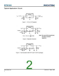
The output voltage is set by the internal feedback resistors when this pin
grounded. If external feedback resistors are applied, the output voltage will be:
ADJ
V
OUT
= 0.8 × (1 + R1 ) Volts
R2
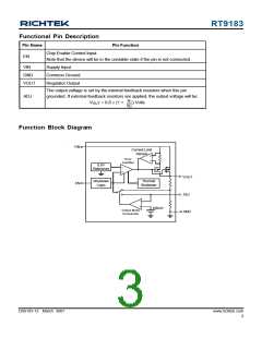
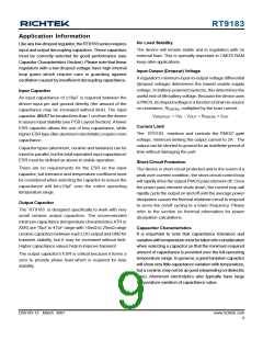
Function Block Diagram
VIN
Current Limit
Sensor
+
-
Error
Amplifier
0.8V
Reference
-
+
VOUT
ADJ
Shutdown
Logic
Thermal
Shutdown
EN
-
+
100mV
Output Mode
Comparator
GND
DS9183-12 March 2007
www.richtek.com
3

 RICHTEK [ RICHTEK TECHNOLOGY CORPORATION ]