RT9173B
Input Capacitor and Layout Consideration
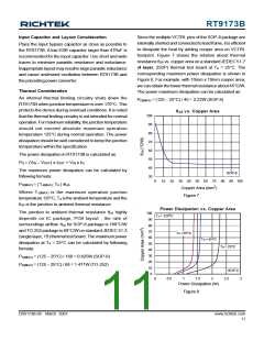
Since the multiple VCTRL pins of the SOP-8 package are
internally shorted and connected to lead frame, it is efficient
to dissipate the heat by adding cooper area on VCTRL
footprint. Figure 7 shows the relation about thermal
resistance θJA vs. copper area on a standard JEDEC 51-7
(4 layer, 2S2P) thermal test board at TA = 25°C. The
corresponding maximum power dissipation is shown in
Figure 8. For example, with 10mm x 10mm cooper area,
we can obtain the lower thermal resistance about 45°C/W.
The power maximum dissipation can be calculated as:
Place the input bypass capacitor as close as possible to
the RT9173B. A low ESR capacitor larger than 470uF is
recommended for the input capacitor. Use short and wide
traces to minimize parasitic resistance and inductance.
Inappropriate layout may result in large parasitic inductance
and cause undesired oscillation between RT9173B and
the preceding power converter.
Thermal Consideration
An internal thermal limiting circuitry shuts down the
RT9173B when junction temperature is over 170°C. This
protects the device during overload conditions. It is noted
that the thermal limiting circuitry is not intended for normal
operation. For maximum reliability, the junction temperature
should not exceed absolute maximum operation
temperature 125°C during normal operation. The power
dissipation should be well considered to keep the junction
temperature within the specification.
PD(MAX) = (125 − 25°C) / 45 = 2.22W (SOP-8)
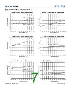
θJA vs. Copper Area
100
90
80
70
60
50
40
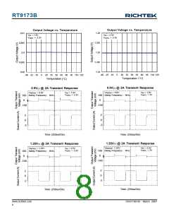
The power dissipation in RT9173B is calculated as:
PD = (VIN − VOUT) x IOUT + VIN x IQ
The maximum power dissipation can be calculated by
following formula:
SOP-8
30
0
10 20 30 40 50 60 70 80 90 100
Copper Area (mm2)
PD(MAX) = ( TJ(MAX) -TA ) /θJA
Where TJ(MAX) is the maximum operation junction
Figure 7
temperature 125°C, TA is the ambient temperature and the
θJA is the junction to ambient thermal resistance.
Power Dissipation vs. Copper Area
The junction to ambient thermal resistance θJA highly
depends on IC package, PCB layout , the rate of
surroundings airflow. θJA for SOP-8 package is 160°C/W
and TO-252 package is 68°C/W on standard JEDEC 51-3
(single layer, 1S) thermal test board. The maximum power
dissipation at TA = 25°C can be calculated by following
formula:
100
90
80
70
60
50
40
30
20
10
0
TJ = 125°C
TA = 65°C
TA = 55°C
TA = 25°C
PD(MAX) = (125 − 25°C) / 160 = 0.625W (SOP-8)
PD(MAX) = (125 − 25°C) / 68 = 1.471W (TO-252)
SOP-8
2.5 3
0
0.5
1
1.5
2
Power Dissipation (W)
Figure 8
DS9173B-09 March 2007
www.richtek.com
11

 RICHTEK [ RICHTEK TECHNOLOGY CORPORATION ]