RT9173B
Absolute Maximum Ratings (Note 1)
z Input Voltage------------------------------------------------------------------------------------------------------------ 7V
z Power Dissipation, PD @ TA = 25°C
SOP-8 -------------------------------------------------------------------------------------------------------------------- 0.625W
TO-252 ------------------------------------------------------------------------------------------------------------------- 1.471W
z Package Thermal Resistance (Note 5)
SOP-8, θJA -------------------------------------------------------------------------------------------------------------- 160°C/W
SOP-8, θJC -------------------------------------------------------------------------------------------------------------- 23°C/W
TO-252, θJA ------------------------------------------------------------------------------------------------------------- 68°C/W
TO-252, θJC ------------------------------------------------------------------------------------------------------------- 8°C/W
z Lead Temperature (Soldering, 10 sec.)--------------------------------------------------------------------------- 260°C
z Junction Temperature ------------------------------------------------------------------------------------------------ 150°C
z Storage Temperature Range ---------------------------------------------------------------------------------------- –65°C to 150°C
z ESD Susceptibility (Note 2)
HBM (Human Body Mode) ------------------------------------------------------------------------------------------ 2kV
MM (Machine Mode) -------------------------------------------------------------------------------------------------- 200V
Recommended Operating Conditions (Note 3)
z Junction Temperature Range---------------------------------------------------------------------------------------- –40°C to 125°C
Electrical Characteristics
(VIN = 2.5V, VCNTL = 3.3V, VREFEN = 1.25V, COUT = 10μF (Ceramic), TA = 25°C unless otherwise specified)
Parameter
Symbol
Test Conditions
Min
Typ
Max Units
Output Offset Voltage
V
IOUT = 0A, Figure 1 (Note 4)
−20
0
20
20
mV
mV
OS
I : 0A → 2A, Figure 1
L
Load Regulation
ΔV
−20
0
LOAD
I : 0A → -2A
L
V
1.7 2.5/1.8
--
6
Keep V
≥ V on operation power
IN
IN
CNTL
Input Voltage Range (DDR I/II)
V
on and power off sequences
No Load
V
3
--
--
3.3/5
1
CNTL
CNTL
SHDN
Operating Current of VCNTL
Current In Shutdown Mode
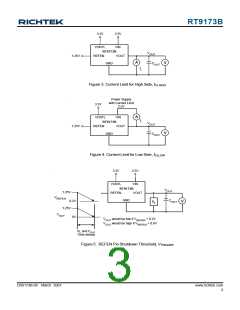
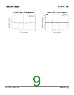
Short Circuit Protection
Current limit
I
I
2.5
90
mA
V
< 0.2V, R = 180Ω, Figure 2
50
μA
REFEN
L
I
Figure 3,4
2.2
2.6
--
A
LIM
Over Temperature Protection
Thermal Shutdown Temperature
Thermal Shutdown Hysteresis
Shutdown Function
T
3.3V ≤ V
≤ 5V
≤ 5V
125
--
170
35
--
--
°C
°C
SD
CNTL
ΔT
3.3V ≤ V
CNTL
SD
Output = High, Figure 5
Output = Low, Figure 5
0.6
--
--
--
--
Shutdown Threshold Trigger
V
0.2
DS9173B-09 March 2007
www.richtek.com
5

 RICHTEK [ RICHTEK TECHNOLOGY CORPORATION ]