RT9164A
Application Information
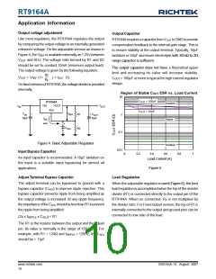
Output voltage adjustment
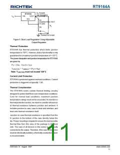
Output Capacitor
Like most regulators, the RT9164A regulates the output
by comparing the output voltage to an internally generated
reference voltage. On the adjustable version as shown in
Figure 4, the VREF is available externally as 1.25V between
VOUT and ADJ. The voltage ratio formed by R1 and R2
should be set to conduct 10mA (minimum output load).
RT9164Arequires a capacitor from VOUT toGNDto provide
compensation feedback to the internal gain stage. This is
to ensure stability at the output terminal. Typically, 10μF
tantalum or 50μF aluminum electrolytic with 30mΩ to 2Ω
range capacitor is sufficient.
The output capacitor does not have a theoretical upper
limit and increasing its value will increase stability.
COUT = 100μF or more is typical for high current regulator
design.
The output voltage is given by the following equation:
R2
VOUT = VREF (1+
) + IADJ R2
R
1
On fixed versions of RT9164A, the voltage divider is provided
internally.
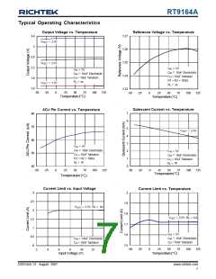
Region of Stable COUT ESR vs. Load Current
10
C
= 100uF
= 10uF
OUT
RT9164A
Instable
VIN
VOUT
ADJ
V
OUT
V
IN
C
OUT
V
C
C
R1
R2
REF
1
0.1
IN
OUT
10uF
10uF
I
ADJ
Stable
65uF
C
ADJ
Figure 4. Basic Adjustable Regulator
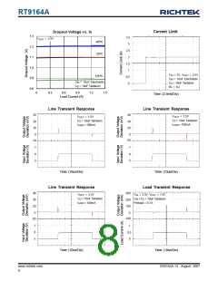
Input Bypass Capacitor
Instable
0.01
0
0.2
0.4
0.6
0.8
1
An input capacitor is recommended. A 10μF tantalum on
the input is a suitable input bypassing for almost all
applications.
Load Current (A)
Figure 5
Adjust Terminal Bypass Capacitor
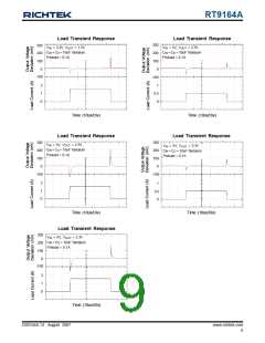
Load Regulation
The adjust terminal can be bypassed to ground with a
bypass capacitor (CADJ) to improve ripple rejection. This
bypass capacitor prevents ripple from being amplified as
the output voltage is increased. At any ripple frequency,
the impedance of the CADJ should be less than R1 to prevent
the ripple from being amplified:
When the adjustable regulator is used (Figure 6), the best
load regulation is accomplished when the top of the resistor
divider (R1) is connected directly to the output pin of the
RT9164A. When so connected, RP is not multiplied by
the divider ratio. For Fixed output version, the top of R1 is
internally connected to the output and ground pins can be
connected to low side of the load.
(2π x fRIPPLE x CADJ) < R1
The R1 is the resistor between the output and the adjust
pin. Its value is normally in the range of 100-200Ω. For
example, with R1 = 124Ω and fRIPPLE = 120Hz, the CADJ
should be > 11μF.
www.richtek.com
10
DS9164A-13 August 2007

 RICHTEK [ RICHTEK TECHNOLOGY CORPORATION ]