RT8841
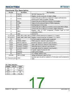
Functional Pin Description
Pin No.
Pin Name
Pin Function
1
2
VIDSEL
VID DAC Selection Pin.
Negative remote sense pin of output voltage.
FBRTN
SS/EN
Connect this pin to GND by a capacitor to adjust soft start time.
Pull this pin to GND to disable controller.
3
4
5
6
7
8
ADJ
COMP
FB
Connect this pin to GND by a resistor to set loadline.
Output of error-amp and input of PWM comparator.
Inverting input of error-amp.
OFS
RT
Connect this pin to GND by a resistor to set no-load offset voltage.
Connect this pin to GND by a resistor to adjust frequency.
Negative input of OCP comparator. (Positive input of OCP
comparator is ADJ).
9
IMAX
GND
10
11,14,15,18
12,13,16,17
19
Ground Pin.
ISP4, ISP3, ISP2, ISP1 Positive current sense pin of channel 1, 2, 3 and 4.
ISN4, ISN3, ISN2, ISN1 Negative current sense pin of channel 1, 2, 3 and 4.
VCC5
5V LDO output for system power supply pin.
PWM output for channel 4 and channel 3.
Bootstrap supply for channel 2 and channel 1.
Upper gate driver for channel 2 and channel 1.
Switching node of channel 2 and channel 1.
Lower gate driver for channel 2 and channel 1.
IC power supply. Connect to 12V.
20,21
22,30
23,29
24,28
25,27
26
PWM4, PWM3
BOOT2, BOOT1
UGATE2, UGATE1
PHASE2, PHASE1
LGATE2, LGATE1
VCC12
31
PWRGD
Power good indicator.
32
EN/VTT
VTT voltage detector input.
33 to 40
VID7 to VID0
Voltage identification input for DAC.
Exposed pad should be soldered to PCB board and connected to
GND.
41 (Exposed pad) GND
VID Table Selection
VIDSEL VID [7]
Table
VTT
GND
VCC5
VCC5
X
X
VR11
VR10.x
K8
VTT
GND
K8_M2
DS8841-01 April 2011
www.richtek.com
17

 RICHTEK [ RICHTEK TECHNOLOGY CORPORATION ]