RT8802A
IOFS
4
L
If
X
= (R //R )× Cx then
X
PX
DCRx
R
PX
VCx =
×I ×DCRx
LX
Rx + R
PX
R
FB1
V
-
CORE
EA
COMP
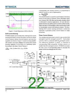
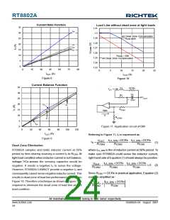
With other phase kept unchanged, this phase would share
(RPX+Rx)/RPX times current than other phases. Figure 6
and 7 show different current ratio setting for the power
stage when Phase 4 is programmed 2 times current than
other phases. Figure 8 and 9 compare the above current
ratio setting results.
+
V
ADJ
4IX
DAC
R
ADJ
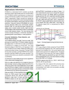
Figure 4. Load Line and Offset Function
Output Voltage Offset Function
L
X
I
DCRx
LX
To meet Intel®requirement of initial offset of load line,
RT8802A provides programmable initial offset function.
External resistor ROFS and voltage source at OFS pin
VOFS
VCx
-
Rx
+
Cx
R
PX
generate offset current IOFS
=
ROFS
, where VOFS is 1V typical. One quarter of IOFS flows
through RFB1 as shown in Figure 4. Error amplifier would
hold the inverting pin equal to VDAC - VADJ. Thus output
voltage is subtracted from VDAC - VADJ for a constant offset
V
OUT
T
voltage.
VCORE = VDAC − VADJ
Figure 5
RFB1
4×ROFS
−
A positive output voltage offset is possible by connecting
ROFS to VDD instead of to GND. Please note that when
ROFS is connected to VDD, VOFS is VDD − 2V typically and
half of IOFS flows through RFB1. VCORE is rewritten as :
RFB1
VCORE = VDAC − VADJ
+
ROFS
Current Ratio Setting
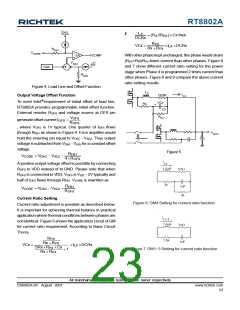
Figure 6. GM4 Setting for current ratio function
Current ratio adjustment is possible as described below.
It is important for achieving thermal balance in practical
application where thermal conditions between phases are
not identical. Figure 5 shows the application circuit ofGM
for current ratio requirement. According to Basic Circuit
Theory
RPX
Rx + RPX
SRx ×RPX × Cx
VCx =
×ILX ×DCRx
Figure 7. GM1~3 Setting for current ratio function
+1
Rx + RPX
All brandname or trademark belong to their owner respectively
DS8802A-04 August 2007
www.richtek.com
23

 RICHTEK [ RICHTEK TECHNOLOGY CORPORATION ]