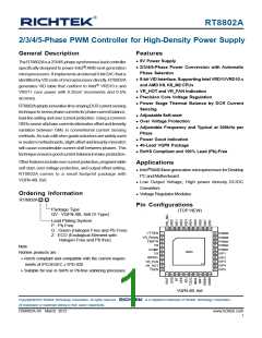
RT8802A
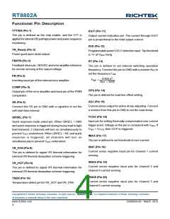
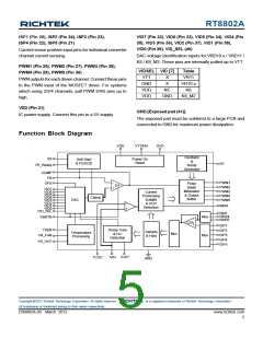
ISP1 (Pin 25), ISP2 (Pin 24), ISP3 (Pin 23),
ISP4 (Pin 22), ISP5 (Pin 21)
VID7 (Pin 32), VID6 (Pin 33), VID5 (Pin 34), VID4 (Pin
35), VID3 (Pin 36), VID2 (Pin 37), VID1 (Pin 38),
VID0 (Pin 39), VID_SEL (40)
Current sense positive input pins for individual converter
channel current sensing.
DAC voltage identification inputs for VRD10.x / VRD11 /
K8 / K8_M2. These pins are internally pulled up to VTT.
PWM1 (Pin 26), PWM2 (Pin 27), PWM3 (Pin 28),
PWM4 (Pin 29), PWM5 (Pin 30)
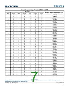
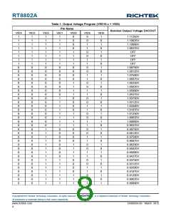
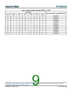
VIDSEL VID [7]
Table
VR11
VR10.x
K8
VTT
GND
VDD
VDD
X
X
PWM outputs for each driven channel. Connect these pins
to the PWM input of the MOSFET driver. For systems
which using 2/3/4 channels, pull PWM 3/4/5 pins up to
high.
NC
GND
K8_M2
VDD (Pin 31)
GND [Exposed pad (41)]
IC power supply. Connect this pin to a 5V supply.
The exposed pad must be soldered to a large PCB and
connected to GND for maximum power dissipation.
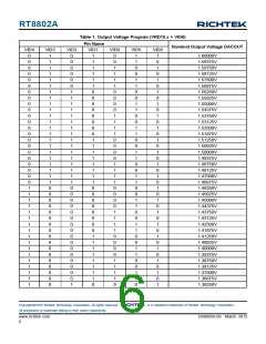
Function Block Diagram
VDD
VTT/EN
DVD
Oscillator
&
Ramp
SS
Power On
Reset
Soft Start
& PGOOD
RT
VR_Ready
Generator
COMP
FB
-
PWM1
PWM2
PWM3
PWM4
PWM5
OFS
Pulse
Width
Modulator
& Output
Buffer
EA
+
VID7
VID6
Current
Processing
SUM/N
& OCP
Detection
VID5
VID4
Clamp
DAC
VID3
VID2
-
+
VID1
IMAX
VID0
VID_SEL
ISN1
ISN24
Mux
Mux
FBRTN
-
ISN35
CSA
+
ISP1
ISP2
ISP3
ISP4
ISP5
TSEN
Droop Tune
& Hi-I
Detection
Sample
& Hold
Temperature
Processing
Mux
VR_FAN
VR_HOT
ADJ IOUT
TCOC
GND
Copyright 2012 Richtek Technology Corporation. All rights reserved.
©
is a registered trademark of Richtek Technology Corporation.
All brandname or trademark belong to their owner respectively.
DS8802A-09 March 2012
www.richtek.com
5

 RICHTEK [ RICHTEK TECHNOLOGY CORPORATION ]