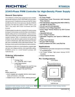
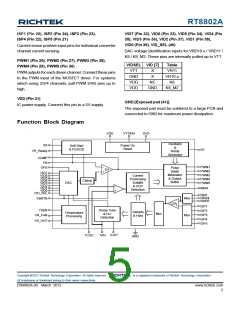
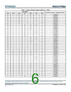
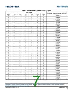
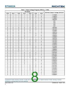
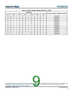
RT8802A
Functional Pin Description
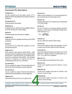
VTT/EN (Pin 1)
IOUT (Pin 11)
The pin is defined as the chip enable, and the VTT is
applied for internal VIDpull high power and power sequence
monitoring.
Output current indication pin. The current through IOUT
pin is proportional to the total output current.
DVD (Pin 12)
VR_Ready (Pin 2)
Programmable power UVLO detection input. Trip threshold
is 1V at VDVD rising.
Power good open-drain output.
FBRTN (Pin 3)
RT (Pin 13)
Feedback return pin. VIDDAC and error amplifier reference
for remote sensing of the output voltage.
The pin is defined to set internal switching operation
frequency. Connect this pin toGNDwith a resistor RRT to
set the frequency FSW
.
FB (Pin 4)
4.463 e9
F
SW
=
Inverting input pin of the internal error amplifier.
R
+ 3500
RT
COMP (Pin 5)
OFS (Pin 14)
Output pin of the error amplifier and input pin of the PWM
comparator.
The pin is defined for load line offset setting.
ADJ (Pin 15)
SS (Pin 6)
Current sense output for active droop adjusting. Connect
a resistor from this pin to GND to set the load droop.
Connect this SS pin to GND with a capacitor to set the
soft-start time interval.
TCOC (Pin 16)
QRSEL (Pin 7)
Input pin for setting thermally compensated over current
trigger point. Voltage on the pin is compared with VADJ. If
VADJ > VTCOC then OCP is triggered.
Quick response mode select pin. When QRSEL = GND
and quick response is triggered during heavy load to light
load transient, 2 channels will turn on simultaneously to
prevent VOUT undershoot. When QRSEL = NC and quick
response is triggered, all channels will turn on
simultaneously to prevent VOUT undershoot.
IMAX (Pin 17)
The pin is defined to set threshold of over current.
ISN1 (Pin 18)
VR_FAN (Pin 8)
Current sense negative input pin for channel 1 current
sensing.
The pin is defined to signal VR thermal information for
external VR thermal dissipation scheme triggering.
ISN24 (Pin 19)
VR_HOT (Pin 9)
Current sense negative input pins for channel 2 and
channel 4 current sensing.
The pin is defined to signal VR thermal information for
external VR thermal dissipation scheme triggering.
ISN35 (Pin 20)
TSEN (Pin 10)
Current sense negative input pins for channel 3 and
channel 5 current sensing.
Temperature detect pin for VR_HOT and VR_FAN.
Copyright 2012 Richtek Technology Corporation. All rights reserved.
©
is a registered trademark of Richtek Technology Corporation.
All brandname or trademark belong to their owner respectively.
www.richtek.com
4
DS8802A-09 March 2012

 RICHTEK [ RICHTEK TECHNOLOGY CORPORATION ]