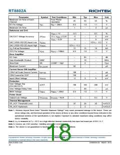
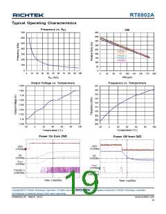
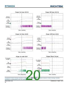
RT8802A
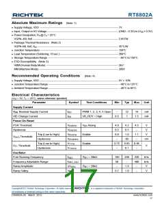
Parameter
Symbol
Test Conditions
Min
Typ
Max
Unit
Maximum On-Time of Each
Channel
Four Phase
Operation
45
50
55
%
RT Pin Voltage
V
RT
R
RT
= 20kΩ
0.9
1
1.0
--
1.1
3
V
Maximum On-Time
Reference and DAC
μs
V
≥ 1V
−0.5
−5
−8
--
--
--
0.5
5
%
mV
mV
V
DAC
DACOUT Voltage Accuracy
ΔV
1V ≥ V
≥ 0.8V
DAC
DAC
V
DAC
< 0.8V
--
8
DAC (VID0-VID125) Input Low
DAC (VID0-VID125) Input High
V
--
1/2V − 0.2
ILDAC
TT
V
IHDAC
1/2V + 0.2
--
--
V
TT
V
Pull-up Resistance
12
15
1.0
18
1.1
kΩ
V
ID
OFS Pin Voltage
V
OFS
R
OFS
= 100kΩ
0.9
Error Amplifier
DC Gain
--
--
65
10
8
--
--
--
--
dB
MHz
V/μs
μA
Gain-Bandwidth Product
Slew Rate
GBW
SR
COMP = 10pF
--
Maximum Current
Current Sense GM Amplifier
CSN Full Scale Source Current
CSN Current for OCP
Input Offset Voltage
Protection
I
50
--
EA_SLEW
I
100
150
−5
--
--
0
--
--
5
μA
μA
ISPFSS
V
OSCS
mV
Over Voltage Trip
(FB-DACOUT)
ΔOVT
100
150
200
mV
Over Voltage Delay Time
IMAX Voltage
--
20
--
μs
V
IMAX
R
IMAX
= 20kΩ
0.9
1.0
1.1
V
Power Good
Output Low Voltage
Thermal Management
VR_HOT Threshold Level
VR_HOT Hysteresis
V
I
= 4mA
--
--
0.2
V
PGOODL
PGOOD
25
--
28
5
30
--
%VCC5
%VCC5
Note 1. Stresses beyond those listed “Absolute Maximum Ratings” may cause permanent damage to the device. These are
stress ratings only, and functional operation of the device at these or any other conditions beyond those indicated in the
operational sections of the specifications is not implied. Exposure to absolute maximum rating conditions may affect
device reliability.
Note 2. θJA is measured at TA = 25°C on a high effective thermal conductivity four-layer test board per JEDEC 51-7.
Note 3. Devices are ESD sensitive. Handling precaution recommended.
Note 4. The device is not guaranteed to function outside its operating conditions.
Copyright 2012 Richtek Technology Corporation. All rights reserved.
©
is a registered trademark of Richtek Technology Corporation.
All brandname or trademark belong to their owner respectively.
www.richtek.com
18
DS8802A-09 March 2012

 RICHTEK [ RICHTEK TECHNOLOGY CORPORATION ]