RT8223P
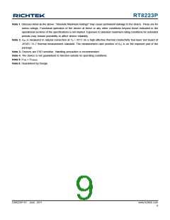
Typical Application Circuit
V
IN
6V to 25V
R8
3.9
C13
C1
0µF
RT8223P
UGATE2
R10
0
C12
10µF
10µF
1
Q2
10
9
16
VIN
BSC119
C10
0.1µF
N03S
0
BOOT2
R
BOOT2
C11
0.1µF
L2
R4 0
4.7µH
21
22
Q1
BSC119
N03S
V
UGATE1
BOOT1
OUT2
11
12
15
PHASE2
LGATE2
GND
3.3V
0
Q4
BSC119
N03S
C17
220µF
R11
C14
R
BOOT1
C2
0.1µF
L1
6.8µH
V
OUT1
5V
20
19
PHASE1
LGATE1
7
5
VOUT2
FB2
Q3
C3
220µF
R5
C4
C21
R14
6.5k
BSC119
R
150k
ILIM1
N03S
1
C20
ENTRIP1
0.1µF
24
R15
10k
R
150k
VOUT1
ILIM2
C18
6
R12
15k
ENTRIP2
GND
2
3
FB1
REF
25 (Exposed Pad)
C19
0.1µF
V
REF
2V
R13
10k
C15
0.22µF
17
VREG5
5V Always On
4
14
13
TONSEL
SKIPSEL
EN
ontrol
Frequency C
C9
R6
100k
4.7µF
sonic
ON
PWM/DEM/Ultra
23
8
PGOOD
VREG3
PGOOD Indicator
3.3V Alwa
ys On
C16
4.7µF
OFF
ON
18
ENC
OFF
Functional Pin Description
Pin No.
Pin Name
Pin Function
Channel 1 Enable and Current Limit Setting Input. Connect a resistor to GND to
set the threshold for channel 1 synchronous RDS(ON) sense. The GND − PHASE1
current limit threshold is 1/10th the voltage seen at ENTRIP1 over a 0.515V to 3V
range. There is an internal 10μA current source from VREG5 to ENTRIP1. Leave
ENTRIP1 floating or short ENTRIP1 to GND to shut down channel 1.
1
ENTRIP1
SMPS1 Feedback Input. Connect FB1 to a resistive voltage divider from VOUT1
to GND to adjust output from 2V to 5.5V.
2
3
FB1
2V Reference Output. Bypass to GND with a minimum 0.22μF capacitor. REF can
source up to 100μA for external loads. Loading REF degrades FBx and output
accuracy according to the REF load-regulation error.
REF
Frequency Selectable Input for VOUT1/VOUT2 respectively.
400kHz/500kHz : Connect to VREG5 or VREG3
300kHz/375kHz : Connect to REF
4
5
TONSEL
FB2
200kHz/250kHz : Connect to GND
SMPS2 Feedback Input. Connect FB2 to a resistive voltage divider from VOUT2
to GND to adjust output voltage from 2V to 5.5V.
Channel 2 Enable and Current Limit Setting Input. Connect a resistor to GND to
set the threshold for channel 2 synchronous RDS(ON) sense. The GND − PHASE2
current limit threshold is 1/10th the voltage seen at ENTRIP2 over a 0.515V to 3V
range. There is an internal 10μA current source from VREG5 to ENTRIP2. Leave
ENTRIP2 floating or short ENTRIP2 to GND to shut down channel 2.
6
ENTRIP2
Bypass Pin for SMPS2. Connect to the SMPS2 output to bypass efficient power
for VREG3 pin. VOUT2 is also for the SMPS2 output soft-discharge.
7
8
VOUT2
VREG3
3.3V Linear Regulator Output.
To be continued
www.richtek.com
2
DS8223P-01 June 2011

 RICHTEK [ RICHTEK TECHNOLOGY CORPORATION ]