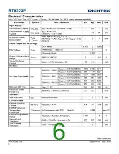
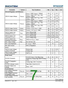
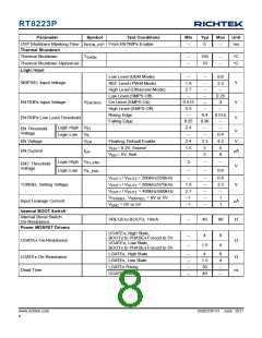
RT8223P
Parameter
Symbol
Test Conditions
Min
Typ
Max
Unit
Internal Regulator and Reference
V
= GND, I
< 100mA
VREG5
4.8
5
5
5.2
OUT1
V
OUT1
= GND, 6.5V < V < 25V,
< 100mA
IN
4.75
5.25
VREG5 Output Voltage
VREG3 Output Voltage
V
V
VREG5
I
VREG5
V
= GND, 5.5V < V < 25V,
< 50mA
OUT1
IN
4.75
3.2
5
5.25
3.46
3.5
I
VREG5
V
OUT2
= GND, I
< 100mA
VREG3
3.33
3.33
V
OUT2
= GND, 6.5V < V < 25V,
IN
3.13
V
V
VREG3
I
< 100mA
VREG3
V
= GND, 5.5V < V < 25V,
< 50mA
OUT2
IN
3.13
3.33
3.5
I
VREG3
VREG5 Output Current
VREG3 Output Current
I
V
= 4.5V, V = GND
OUT1
100
100
4.6
4.3
175
175
4.75
4.4
250
250
4.9
mA
mA
VREG5
VREG5
I
V
= 3V, V
= GND
OUT2
VREG3
VREG3
V
OUT1
Rising Edge
Falling Edge
Rising Edge
Falling Edge
VREG5 Switch-over
V
V
SW5
Threshold to V
OUT1
V
OUT1
4.5
V
OUT2
2.975 3.125 3.25
2.775 2.875 2.975
VREG3 Switch-over
Threshold to V
V
V
SW3
OUT2
V
OUT2
VREGx Switch-over
Equivalent Resistance
R
SWx
VREGx to V , 10mA
OUTx
--
1.5
3
Ω
REF Output Voltage
REF Load Regulation
REF Sink Current
UVLO
V
REF
No External Load
0 < I < 100μA
1.98
--
2
10
--
2.02
--
V
mV
μA
LOAD
REF in Regulation
5
--
Rising Edge
Falling Edge
--
4.2
3.9
4.45
4.1
VREG5 Under Voltage
Lockout Threshold
V
V
3.7
VREG3 Under Voltage
Lockout Threshold
SMPSx off
--
2.5
--
Power Good
PGOOD Detect, FBx falling Edge
82
--
85
6
88
--
PGOOD Threshold
%
Hysteresis, Rising Edge with SS Delay
Time
PGOOD Propagation
Delay
Falling Edge, 50mV Overdrive
High State, Forced to 5.5V
--
--
--
10
--
--
1
μs
μA
V
PGOOD Leakage Current
PGOOD Output Low
Voltage
I
= 4mA
--
0.3
SINK
Fault Detection
Over Voltage Protection
Trip Threshold
Over Voltage Protection
Propagation Delay
V
OVP Detect, FBx Rising Edge
FBx = 2.35V
109
--
112
5
116
--
%
μs
%
FB_OVP
Under Voltage Protection
Trip Threshold
V
UVP Detect, FBx Falling Edge
49
52
56
FB_UVP
To be continued
DS8223P-01 June 2011
www.richtek.com
7

 RICHTEK [ RICHTEK TECHNOLOGY CORPORATION ]