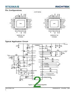
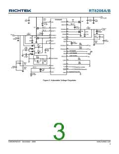
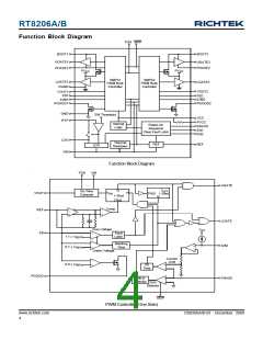
RT8206A/B
BOOT1 (Pin 17)
PHASE2 (Pin 25)
Boost Flying Capacitor Connection for SMPS1. Connect
to an external capacitor according to the typical application
circuits.
Inductor Connection for SMPS2. PHASE2 is the internal
lower supply rail for the UGATE2 high-side gate driver.
PHASE2 is the current-sense input for the SMPS2.
LGATE1 (Pin 18)
UGATE2 (Pin 26)
SMPS1 Synchronous-RectifierGate-drive Output. LGATE1
swings between PGNDand PVCC.
High-Side MOSFET Floating Gate-Driver Output for
SMPS2. UGATE2 swings between PHASE2 and BOOT2.
PVCC (Pin 19)
EN2 (Pin 27)
PVCC is the supply voltage for the low-side MOSFET
driver LGATEx. Connect a 5V power source to the PVCC
pin (bypass with 1uF MLCC capacitor to PGND if
necessary). There is an internal 10Ω connecting from
PVCC to VCC. Make sure that both VCC and PVCC are
bypassed with 1uF MLCC capacitors.
SMPS2 Enable Input. The SMPS2 will be enabled if EN2
is greater than the logic high level and be disabled if EN2
is less than the logic low level. If EN2 is connected to
REF, the SMPS2 starts after the SMPS1 reaches
regulation (delay start). Drive EN2 below 0.8V to clear
fault level and reset the fault latches.
SECFB (Pin 20) (RT8206A)
PGOOD2 (Pin 28)
The SECFB is used to monitor the optional external 14V
charge pump. Connect a resistive voltage-divider from the
14V charge pump output to GND to detect the output. If
SECFB drops below the threshold voltage, LGATE1 will
be turned on for 300ns. This will refresh the external charge
pump driven by LGATE1 without over-discharging the
output voltage.
SMPS2 Power-Good Open-Drain Output. PGOOD2 is low
when the SMPS2 output voltage is more than 7.5% below
the normal regulation point or during soft-start. PGOOD2
is high impedance when the output is in regulation and
the soft-start circuit has terminated. PGOOD2 is low in
shutdown.
SKIP (Pin 29)
NC (Pin 20) (RT8206B)
SMPS Operation Mode Control.
No Internal Connection.
SKIP = GND : DEM operation
SKIP = REF : Ultrasonic Mode operation
SKIP = VCC : PWM operation.
GND [Pin 21, Exposed Pad (33)]
Analog Ground for both SMPS and LDO. The exposed
pad must be soldered to a large PCB and connected to
GND for maximum power dissipation.
VOUT2 (Pin 30)
SMPS2 Output Voltage-Sense Input. Connect this pin to
the SMPS2 output. VOUT2 is an input to the constant
on-time-PWM one-shot circuit. It also serves as the
SMPS2 feedback input in fixed-voltage mode.
PGND (Pin 22)
Power Ground for SMPS controller. Connect PGND
externally to the underside of the exposed pad.
LGATE2 (Pin 23)
ILIM2 (Pin 31)
SMPS2 Synchronous-RectifierGate-drive Output. LGATE2
swings between PGNDand PVCC.
SMPS2 Current-Limit Adjustment. The GND − PHASE2
current-limit threshold is 1/10th the voltage seen at ILIM2
over a 0.5V to 2V range. There is an internal 5uA current
source from VCC to ILIM2. The logic current limit threshold
is default to 100mV value if ILIM2 is higher than (VCC −
1V).
BOOT2 (Pin 24)
Boost Flying Capacitor Connection for SMPS2. Connect
this pin to an external capacitor according to the typical
application circuits.
www.richtek.com
6
DS8206A/B-03 December 2009

 RICHTEK [ RICHTEK TECHNOLOGY CORPORATION ]