RT7274/79/80/81
be taken when these capacitors are used at input and
output. When a ceramic capacitor is used at the input
and the power is supplied by a wall adapter through long
wires, a load step at the output can induce ringing at the
input, VIN. A sudden inrush of current through the long
wires can potentially cause a voltage spike at VIN large
enough to damage the part.
Under Voltage Protection
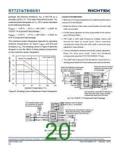
Latch-Off Mode (RT7279/80)
For the RT7279GCP/RT7280GCP, it provides Latch-Off
Mode Under Voltage Protection (UVP). When the FB pin
voltage drops below 70% of the feedback threshold voltage,
UVP will be triggered and the RT7279GCP/RT7280GCP
will shutdown in Latch-Off Mode. In shutdown condition,
the RT7279GCP/RT7280GCP can be reset by the ENpin
or power input, VIN.
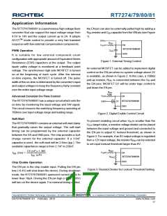
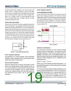
External Bootstrap Diode
Connect a 0.1μF low ESR ceramic capacitor between the
BOOT and SW pins. This capacitor provides the gate driver
voltage for the high side MOSFET. It is recommended to
add an external bootstrap diode between an external 5V
and the BOOT pin for efficiency improvement when input
voltage is lower than 5.5V or duty ratio is higher than 65%.
The bootstrap diode can be a low cost one such as 1N4148
or BAT54. The external 5V can be a 5V fixed input from
system or a 5V output of the RT7274/79/80/81. Note that
the external boot voltage must be lower than 5.5V
5V
Latch-Mode
VLX
(10V/Div)
VOUT
(1V/Div)
ILX
(2A/Div)
Time (1ms/Div)
BOOT
RT7274/79/80/81
0.1µF
Thermal Considerations
SW
For continuous operation, do not exceed absolute
maximum junction temperature. The maximum power
dissipation depends on the thermal resistance of the IC
package, PCB layout, rate of surrounding airflow, and
difference between junction and ambient temperature. The
maximum power dissipation can be calculated by the
following formula :
Figure 5. External Bootstrap Diode
PVCC Capacitor Selection
Decouple with a 1μF ceramic capacitor. X7R or X5R grade
dielectric ceramic capacitors are recommended for their
stable temperature characteristics.
PD(MAX) = (TJ(MAX) − TA) / θJA
Over Current Protection
where TJ(MAX) is the maximum junction temperature, TA is
the ambient temperature, and θJA is the junction to ambient
thermal resistance.
When the output shorts to ground, the inductor current
decays very slowly during a single switching cycle. An
over current detector is used to monitor inductor current
to prevent current runaway. The over current detector
monitors the voltage between SW and GND during the
low side MOS turn-on state. This is cycle-by-cycle
protection.
For recommended operating condition specifications, the
maximum junction temperature is 125°C. The junction to
ambient thermal resistance, θJA, is layout dependent. For
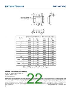
TSSOP-14 (Exposed Pad) package, the thermal
resistance, θJA, is 40°C/W on a standard JEDEC 51-7
four-layer thermal test board. For SOP-8 (Exposed Pad)
Copyright 2013 Richtek Technology Corporation. All rights reserved.
©
is a registered trademark of Richtek Technology Corporation.
DS7274/79/80/81-01 February 2013
www.richtek.com
19

 RICHTEK [ RICHTEK TECHNOLOGY CORPORATION ]