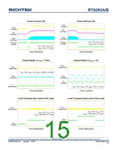
RT6263A/B
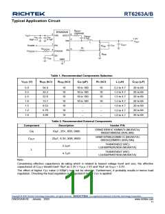
Typical Application Circuit
R
BOOT
RT6263A/B
(Optional)
3
8
2
V
VIN
BOOT
IN
C
0.1μF
BOOT
C
C
IN
IN
1.2V
10μF x 2
0.1μF
SW
V
OUT
L
7
C
OUT
C
FF
Enable
EN
R
FB1
R
T
R
6
PGOOD
4
5
FB
V
PGOOD
SS
PGOOD
R
FB2
C
SS
GND
1
Table 1. Recommended Components Selection
VOUT (V)
RFB1 (k)
RFB2 (k)
CFF (pF)
RT (k)
L (H)
COUT (F)
5.0
3.3
2.5
1.8
1.5
1.2
1.0
54.9
33.2
22.6
13.7
9.53
5.76
3.09
10
10
10
10
10
10
10
10 to 100
10 to 100
10 to 100
10 to 100
--
10
10
10
10
--
2.2 to 4.7
1.5 to 4.7
1.5 to 4.7
1.5 to 4.7
1.0 to 4.7
1.0 to 4.7
1.0 to 4.7
20 to 68
20 to 68
20 to 68
20 to 68
20 to 68
20 to 68
20 to 68
--
--
--
--
Table 2. Recommended External Components
Component
Description
Vendor P/N
GRM21BR61E106MA73 (MURATA)
0805X106M250 (WALSIN)
CIN
10F, 25V, X5R, 0805
GRM187R60J226ME15 (MURATA)
0603X226M6R3 (WALSIN)
COUT
22F, 6.3V, X5R, 0603
74404054022 (WE)
LQH5BPN2R2N38 (MURATA)
2.2H
4.7H
L
74404054047 (WE)
LQH5BPN4R7N38 (MURATA)
Note :
Considering effective capacitance de-rating which is related to biased voltage level and size, the effective
capacitance of COUT should meet 18F as 3.3V ≤ VOUT ≤ 5V and 16F as VOUT < 3.3V.
The effect of higher CFF value (>100pF) may not be obvious. Furthermore, it probably results in worse load
regulation. Checking the load regulation is suggested if higher CFF is applied.
Copyright © 2020 Richtek Technology Corporation. All rights reserved.
is a registered trademark of Richtek Technology Corporation.
DS6263A/B-00 January 2020
www.richtek.com
11

 RICHTEK [ RICHTEK TECHNOLOGY CORPORATION ]