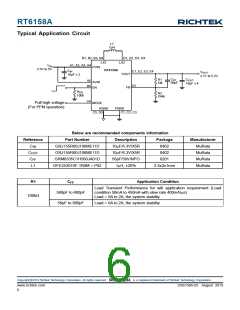
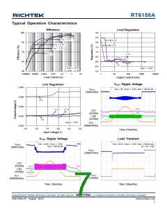
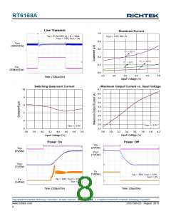
RT6158A
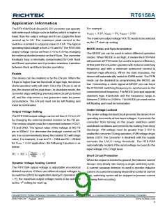
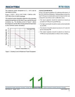
The maximum power dissipation at TA = 25°C can be
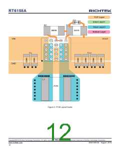
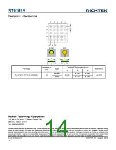
Layout Considerations
calculated as below :
Some PCB layout guidelines for optimal performance of
the RT6158Alist as following. Following figure shows the
real PCB layout considerations and it is based on the real
component size whose unit is millimeter (mm).
PD(MAX) = (125°C − 25°C) / (35.7°C/W) = 2.8W for a WL-
CSP-25B 2.07x2.33 (BSC) package.
The maximum power dissipation depends on the operating
ambient temperature for the fixed TJ(MAX) and the thermal
resistance, θJA. The derating curves in Figure 1 allows
the designer to see the effect of rising ambient temperature
on the maximum power dissipation.
The input capacitor should be placed as closed as
possible to PVIN pin for good filtering.
The high current path should be made as short and wide
as possible.
The inductor should be placed as close to LX1 and LX2
4.0
Four-Layer PCB
pin for reducing EMI.
3.6
3.2
2.8
2.4
2.0
1.6
1.2
0.8
0.4
0.0
The output capacitor should be placed as closed as
PGND pin to ground plane to reduce noise coupling.
0
25
50
75
100
125
Ambient Temperature (°C)
Figure 1. Derating Curve of Maximum PowerDissipation
Copyright 2019 Richtek Technology Corporation. All rights reserved.
©
is a registered trademark of Richtek Technology Corporation.
DS6158A-05 August 2019
www.richtek.com
11

 RICHTEK [ RICHTEK TECHNOLOGY CORPORATION ]