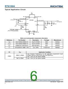
RT6158A
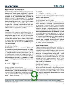
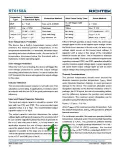
Protection
Type
Threshold Refer
to Electrical Spec.
Protection Method
Shut Down Delay Time
Reset Method
IL < 4.5A
CL will trigger right
away.
OCP
IL > 4.5A
Turn on B, D MOS
UVLO
OTP
VIN < 2.05V
Shutdown
100s
VIN > 2.15V
TEMP > 160°C
Shutdown
No delay
No delay
No delay
OTP Hysteresis = 20°C
VOUT < 5.3V
Output OVP VOUT > 5.6V
SCP VOUT < 1.2V
Stop switching
fSW become 1/4
After FAULT 40ms
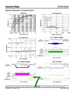
If the RT6158A operates in Buck mode, the worst-case
voltage ripple occurs at the highest input voltage. When
the Buck-boost operates in Boost mode, the worst-case
voltage ripple occurs at the lowest input voltage. A
capacitor with a value in the range of the calculated
minimum should be used. This is required to maintain
control loop stability. There are no additional requirements
regarding minimum ESR. Low ESR capacitors should be
used to minimize output voltage ripple. Larger capacitors
will cause lower output voltage ripple as well as lower
output voltage drop during load transients.
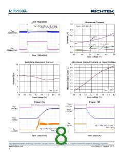
Over-Temperature Protection
The device has a built-in temperature sensor which
monitors the internal junction temperature. If the
temperature exceeds the OTP threshold, the device stops
operating and enters shutdown mode. As soon as the IC
temperature decreases below the threshold with a
hysteresis, it starts operating again.
Over-Voltage Protection
When the VOUT pin is floating, the device will trigger the
over-voltage protection to avoid the output voltage
exceeding critical values for device. In case it reaches the
OVP threshold, the device will regulate the output voltage
to this value.
Thermal Considerations
The junction temperature should never exceed the
absolute maximum junction temperature TJ(MAX), listed
under Absolute Maximum Ratings, to avoid permanent
damage to the device. The maximum allowable power
dissipation depends on the thermal resistance of the IC
package, the PCB layout, the rate of surrounding airflow,
and the difference between the junction and ambient
temperatures. The maximum power dissipation can be
calculated using the following formula :
Inductor Selection
The recommended power inductor is 1μH with over 4.5A
saturation current rating. In applications, it needs to select
an inductor with the low DCR for good performance and
efficiency.
Input and Output Capacitor Selection
The input and output capacitors should be ceramic X5R
type with low ESL and ESR. The recommended input
capacitor value is 2 x 10μF. The recommended output
capacitor value is 4 x 10μF.
PD(MAX) = (TJ(MAX) − TA) / θJA
where TJ(MAX) is the maximum junction temperature, TA is
the ambient temperature, and θJA is the junction-to-ambient
thermal resistance.
The output capacitor selection determines the output
voltage ripple and transient response. It is recommended
to use ceramic capacitors placed as close as possible to
the VOUT and GND pins of the IC. If, for any reason, the
application requires the use of large capacitors which
cannot be placed close to the IC, using a small ceramic
capacitor in parallel to the large one is recommended.
This small capacitor should be placed as close as possible
to the VOUT and GND pins of the IC.
For continuous operation, the maximum operating junction
temperature indicated under Recommended Operating
Conditions is 125°C. The junction-to-ambient thermal
resistance, θJA, is highly package dependent. For a WL-
CSP-25B 2.07x2.33 (BSC) package, the thermal
resistance, θJA, is 35.7°C/W on a standard JEDEC 51-7
high effective-thermal-conductivity four-layer test board.
Copyright 2019 Richtek Technology Corporation. All rights reserved.
©
is a registered trademark of Richtek Technology Corporation.
www.richtek.com
10
DS6158A-05 August 2019

 RICHTEK [ RICHTEK TECHNOLOGY CORPORATION ]