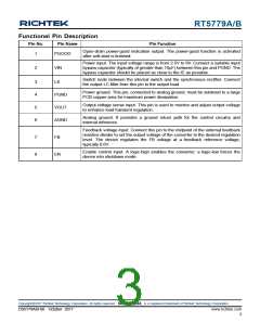
RT5779A/B
Absolute Maximum Ratings (Note 1)
Supply Input Voltage, VIN ----------------------------------------------------------------------------------------- −0.3V to 7V
LX Pin Switch Voltage ---------------------------------------------------------------------------------------------- −0.3V to (VIN + 0.3V)
<10ns ------------------------------------------------------------------------------------------------------------------ −5V to 8.5V
Other Pins------------------------------------------------------------------------------------------------------------- −0.3V to (VIN + 0.3V)
PowerDissipation, PD @ TA = 25°C
TSOT-23-8 (FC) ------------------------------------------------------------------------------------------------------ 1.46W
Package Thermal Resistance (Note 2)
TSOT-23-8 (FC), θJA ------------------------------------------------------------------------------------------------- 68.2°C/W
TSOT-23-8 (FC), θJC ------------------------------------------------------------------------------------------------ 17.1°C/W
Junction Temperature ----------------------------------------------------------------------------------------------- 150°C
Lead Temperature (Soldering, 10 sec.)------------------------------------------------------------------------- 260°C
Storage Temperature Range -------------------------------------------------------------------------------------- −65°C to 150°C
ESD Susceptibility (Note 3)
HBM (Human Body Model)---------------------------------------------------------------------------------------- 2kV
Recommended Operating Conditions (Note 4)
Supply Input Voltage, VIN ----------------------------------------------------------------------------------------- 2.5V to 6V
Junction Temperature Range-------------------------------------------------------------------------------------- −40°C to 125°C
Ambient Temperature Range-------------------------------------------------------------------------------------- −40°C to 85°C
Electrical Characteristics
(VIN = 5V, TA = 25°C, unless otherwise specified)
Parameter
Supply Voltage
Symbol
Test Conditions
Min
Typ
Max Unit
Input Operating Voltage
VIN
2.5
--
6
V
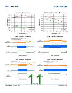
Under-Voltage Lockout
Threshold
VUVLO
2.15
2.3
2.45
Under-Voltage Lockout
Threshold Hysteresis
∆VUVLO
ISHDN
IQ
--
260
--
mV
A
A
Shutdown Current
Quiescent Current
Enable Voltage
VEN = 0V
RT5779A
RT5779B
--
--
--
0
1
50
--
35
600
VENH
VENL
VEN rising
1.2
--
--
--
--
0.4
--
Enable Threshold Voltage
V
VEN falling
EN = 2V
V
--
1.5
0
Enable Input Current
IIH
A
VEN = 0V
--
--
Feedback Voltage
Feedback Input Current
Feedback Voltage
IFB
VFB = 0.6V
--
10
--
nA
V
VFB
0.588 0.6 0.612
Copyright 2017 Richtek Technology Corporation. All rights reserved.
©
is a registered trademark of Richtek Technology Corporation.
DS5779A/B-00 October 2017
www.richtek.com
7

 RICHTEK [ RICHTEK TECHNOLOGY CORPORATION ]