RT5779A/B
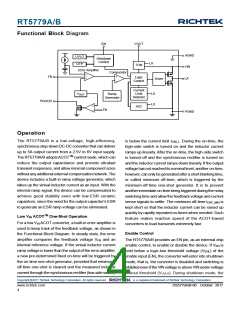
Functional Block Diagram
EN
VOUT
TON
AGND
VIN
UVLO
OTP
Shutdown
Control
LX
Error Amplifier
Comparator
+
-
+
+
-
FB
Logic
Control
LX
Driver
Current
Limit
Detector
LX
V
REF
Ramp
Generator
PGOOD
+
-
LX
AZC
FB
PGND
Operation
The RT5779A/B is a low-voltage, high-efficiency,
synchronous step-downDC-DC converter that can deliver
up to 5A output current from a 2.5V to 6V input supply.
The RT5779A/B adoptsACOTTM control mode, which can
reduce the output capacitance and provide ultrafast
transient responses, and allow minimal component sizes
without any additional external compensation network. The
device includes a built-in ramp voltage generator, which
takes up the virtual inductor current as an input. With the
internal ramp signal, the device can be compensated to
achieve good stability even with low-ESR ceramic
capacitors, since the need for the output capacitor's ESR
to generate an ESR ramp voltage can be eliminated.
is below the current limit ILIM_L. During the on-time, the
high-side switch is turned on and the inductor current
ramps up linearly. After the on-time, the high-side switch
is turned off and the synchronous rectifier is turned on
and the inductor current ramps down linearly. If the output
voltage has not reached its nominal level, another on-time,
however, can only be generated after a short blanking time,
or called minimum off-time, which is triggered by the
minimum-off-time one-shot generator. It is to prevent
another immediate on-time being triggered during the noisy
switching time and allow the feedback voltage and current
sense signals to settle. The minimum off-time tOFF_MIN is
kept short so that the inductor current can be raised up
quickly by rapidly repeated on-times when needed. Such
feature makes reaction speed of the ACOT-based
converters to load transients extremely fast.
Low VIN ACOTTM One-Shot Operation
For a low VIN ACOT converter, a built-in error amplifier is
used to keep track of the feedback voltage, as shown in
the Functional Block Diagram. In steady state, the error
amplifier compares the feedback voltage VFB and an
internal reference voltage. If the virtual inductor current
ramp voltage is lower than the output of the error amplifier,
a new pre-determined fixed on-time will be triggered by
the on-time one-shot generator, provided that minimum-
off-time one-shot is cleared and the measured inductor
current through the synchronous rectifier (low-side switch)
Enable Control
The RT5779A/B provides an EN pin, as an external chip
enable control, to enable or disable the device. If VEN is
held below a logic-low threshold voltage (VENL) of the
enable input (EN), the converter will enter into shutdown
mode, that is, the converter is disabled and switching is
inhibited even if the VIN voltage is above VIN under-voltage
lockout threshold (VUVLO). During shutdown mode, the
Copyright 2017 Richtek Technology Corporation. All rights reserved.
©
is a registered trademark of Richtek Technology Corporation.
www.richtek.com
4
DS5779A/B-00 October 2017

 RICHTEK [ RICHTEK TECHNOLOGY CORPORATION ]