RT2519W
Application Information
The RT2519W is a low voltage, low dropout linear regulator
with input voltage from 2.2V to 6V and a fixed output voltage
from 0.8V to 5.5V.
current limit circuitry controls the pass transistor's gate
voltage to limit the output within the predefined range. By
reason of the build-in body diode, the pass transistor
conducts current when the output voltage exceeds input
voltage. Since the current is not limited, external current
protection should be added if device may work at reverse
voltage state.
Dropout Voltage
The dropout voltage refers to the voltage difference between
the VINand VOUT pins while operating at specific output
current. The dropout voltage VDO also can be expressed
as the voltage drop on the pass-FET at specific output
current(IRATED) while the pass-FET is fully operating at
ohmic region and the pass-FET can be characterized as
an resistance RDS(ON). Thus the dropout voltage can be
defined as (VDO = VVIN − VVOUT = RDS(ON) x IRATED).
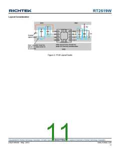
CIN and COUT Selection
Like any low dropout regulator, the external capacitors of
the RT2519W must be carefully selected for regulator
stability and performance. Using a capacitor of at least
4.7μF is suitable. The input capacitor must be located at
a distance of no more than 0.5 inch from the input pin of
the chip. Any good quality ceramic capacitor can be used.
However, a capacitor with larger value and lower ESR
(Equivalent Series Resistance) is recommended since it
will provide better PSRR and line transient response.
For normal operation, the suggested LDO operating range
is (VVIN > VVOUT + VDO) for good transient response and
PSRR ability. Vice versa, while operating at the ohmic
region will degrade these performance severely.
Output Voltage Setting
The RT2519W is designed specifically to work with low
ESR ceramic output capacitor for space saving and
performance consideration. Using a ceramic capacitor with
capacitance of at least 4.7μF on the RT2519W output
ensures stability.
For the RT2519W, the voltage on the FB pin sets the
output voltage and is determined by the values of R1 and
R2. The values of R1 and R2 can be calculated for any
voltage using the formula given in Equation :
R1 + R2
0.8
VOUT
=
Output Noise
R2
Generally speaking, the dominant noise source is from
the internal bandgap for most LDOs. With the noise
reduction capacitor connecting to the NR pin of the
RT2519W, the noise component contributed from bandgap
will not be significantly. Instead, the most noise source
comes from the output resistor divider and the error
amplifier input. For general application to minimize noise,
using a 0.01μF noise-reduction capacitor (CNR) is
recommended.
Using lower values for R1 and R2 is recommended to
reduces the noise injected from the FB pin. Note that R1
is connected from VOUT pin to FB pin, and R2 is
connected from FB to GND.
Chip Enable Operation
The EN pin is the chip enable input. Pull the EN pin low
(<0.4V) will shutdown the device.During shutdown mode,
the RT2519W quiescent current drops to lower than 2μA.
Drive the EN pin to high (>1.2V, <6V) will turn on the
device again. For external timing control (e.g.RC),the EN
pin can also be externally pulled to High by adding a 100kΩ
or greater resistor from the VIN pin.
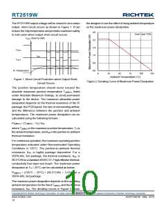
Thermal Considerations
Thermal protection limits power dissipation in the
RT2519W. When the operation junction temperature
exceeds 160°C, the OTP circuit starts the thermal
shutdown function and turns the pass element off. The
pass element turns on again after the junction temperature
cools down by 20°C.
Current Limit
The RT2519W continuously monitors the output current
to protect the pass transistor against abnormal operations.
When an overload or short circuit is encountered, the
Copyright 2019 Richtek Technology Corporation. All rights reserved.
©
is a registered trademark of Richtek Technology Corporation.
DS2519W-00 May 2019
www.richtek.com
9

 RICHTEK [ RICHTEK TECHNOLOGY CORPORATION ]