RT2519W
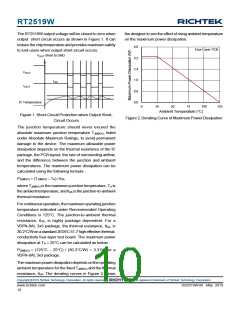
The RT2519W output voltage will be closed to zero when
output short circuit occurs as shown in Figure 1. It can
reduce the chip temperature and provides maximum safety
to end users when output short circuit occurs.
the designer to see the effect of rising ambient temperature
on the maximum power dissipation.
4.0
Four-Layer PCB
V
Short to GND
OUT
3.2
2.4
1.6
0.8
0.0
V
OUT
ILIM’
I
OUT
IC Temperature
0
25
50
75
100
125
Ambient Temperature (°C)
Figure 1. Short-Circuit Protection when Output Short-
Circuit Occurs
Figure 2.Derating Curve of Maximum PowerDissipation
The junction temperature should never exceed the
absolute maximum junction temperature TJ(MAX), listed
under Absolute Maximum Ratings, to avoid permanent
damage to the device. The maximum allowable power
dissipation depends on the thermal resistance of the IC
package, the PCB layout, the rate of surrounding airflow,
and the difference between the junction and ambient
temperatures. The maximum power dissipation can be
calculated using the following formula :
PD(MAX) = (TJ(MAX) − TA) / θJA
where TJ(MAX) is the maximum junction temperature, TA is
the ambient temperature, and θJA is the junction-to-ambient
thermal resistance.
For continuous operation, the maximum operating junction
temperature indicated under Recommended Operating
Conditions is 125°C. The junction-to-ambient thermal
resistance, θJA, is highly package dependent. For a
VDFN-8AL 3x3 package, the thermal resistance, θJA, is
30.2°C/Won a standard JEDEC 51-7 high effective-thermal-
conductivity four-layer test board. The maximum power
dissipation at TA = 25°C can be calculated as below :
PD(MAX) = (125°C − 25°C) / (30.2°C/W) = 3.31W for a
VDFN-8AL 3x3 package.
The maximum power dissipation depends on the operating
ambient temperature for the fixed TJ(MAX) and the thermal
resistance, θJA. The derating curves in Figure 2 allows
Copyright 2019 Richtek Technology Corporation. All rights reserved.
©
is a registered trademark of Richtek Technology Corporation.
www.richtek.com
10
DS2519W-00 May 2019

 RICHTEK [ RICHTEK TECHNOLOGY CORPORATION ]