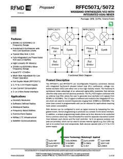
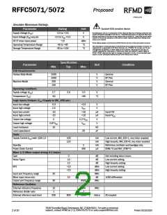
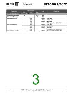
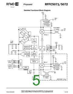
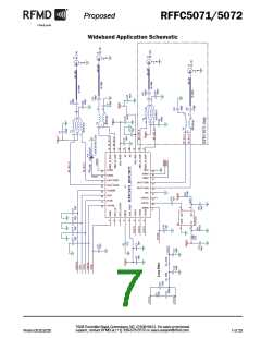
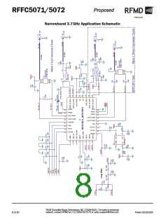
Proposed
RFFC5071/5072
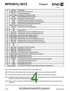
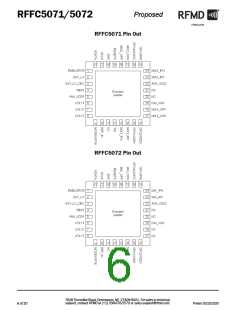
Pin
1
2
Function
ENBL/GPO5
EXT_LO
Description
Device Enable pin. See note 1 and 2.
External local oscillator input.
Decoupling pin for external local oscillator.
External bandgap bias resistor. See note 3.
Analog supply. Use good RF decoupling.
3
4
5
6
7
8
9
EXT_LO_DEC
REXT
ANA_VDD1
LFILT1
LFILT2
LFILT3
MODE/GPO6
REF_IN
Phase detector output. Low-frequency noise-sensitive node.
Loop filter op-amp output. Low-frequency noise-sensitive node.
VCO control input. Low-frequency noise-sensitive node.
Mode select pin. See note 1 and 2.
Reference input. Use AC coupling capacitor.
10
11
12
13
14
15
16
17
18
19
20
21
22
23
24
25
26
27
28
29
30
31
32
NC
TM
Connect to ground.
Differential input 1 (see note 4). On RFFC5072 this pin is NC.
Differential input 1 (see note 4). On RFFC5072 this pin is NC.
General purpose output / MultiSlice address bit.
MIX1_IPN
MIX1_IPP
GPO1/ADD1
GPO2/ADD2
MIX1_OPN
MIX1_OPP
DIG_VDD
NC
General purpose output / MultiSlice address bit.
Differential output 1 (see note 5). On RFFC5072 this pin is NC.
Differential output 1 (see note 5). On RFFC5072 this pin is NC.
Digital supply. Should be decoupled as close to the pin as possible.
NC
Analog supply. Use good RF decoupling.
ANA_VDD2
MIX2_IPP
MIX2_IPN
GPO3/FM
GPO4/LD/DO
MIX2_OPN
MIX2_OPP
RESETX
Differential input 2 (see note 4).
Differential input 2 (see note 4).
General purpose output / frequency control input.
General purpose output / Lock detect output / serial data out.
Differential output 2 (see note 5).
Differential output 2 (see note 5).
Chip reset (active low). Connect to DIG_VDD if asynchronous reset is not required.
Serial interface select (active low). See note 1.
Serial interface clock. See note 1.
ENX
SCLK
SDATA
Serial interface data. See note 1.
Ground reference, should be connected to PCB ground through a low impedance path.
Exposed paddle
Note 1: An RC low-pass filter could be used on this line to reduce digital noise.
Note 2: If the device is under software control this input can be configured as a general purpose output (GPO).
Note 3: Connect a 51K resistor from this pin to ground. This pin is sensitive to low frequency noise injection.
Note 4: DC voltage should not be applied to this pin. Use either an AC coupling capacitor as part of lumped element matching
network or a transformer (see evaluation board schematic).
Note 5: This pin must be connected to ANA_VDD2 using an RF choke or center-tapped transformer (see evaluation board
schematic).
7628 Thorndike Road, Greensboro, NC 27409-9421 · For sales or technical
support, contact RFMD at (+1) 336-678-5570 or sales-support@rfmd.com.
4 of 20
Prelim DS101020

 RFMD [ RF MICRO DEVICES ]