X9313
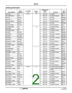
Ordering Information (Continued)
TEMPERATURE
RANGE
PART
V
RANGE
(V)
R
PKG.
DWG. #
CC
TOTAL
(kΩ)
PART NUMBER
MARKING
X9313W D
X9313W ZD
13ZD
(°C)
PACKAGE
8 Ld SOIC
,
X9313WS-3* **
3 to 5.5
10
0 to +70
0 to +70
0 to +70
0 to +70
-40 to +85
-40 to +85
0 to +70
0 to +70
0 to +70
0 to +70
-40 to +85
-40 to +85
MDP0027
M8.15
X9313WSZ-3* (Note)
X9313ZM-3*
8 Ld SOIC (Pb-free)
8 Ld MSOP
1
M8.118
X9313ZMZ-3* (Note)
X9313ZMI-3*
DDK
8 Ld MSOP (Pb-free)
8 Ld MSOP
M8.118
13ZE
M8.118
X9313ZMIZ-3* (Note)
X9313ZP-3
13ZEZ
8 Ld MSOP (Pb-free)
8 Ld PDIP
M8.118
X9313ZP D
X9313ZP ZD
X9313Z D
X9313Z ZD
X9313Z E
X9313Z ZE
MDP0031
MDP0031
MDP0027
M8.15
X9313ZPZ-3 (Note)
8 Ld PDIP (Pb-free)***
8 Ld SOIC
,
X9313ZS-3* **
X9313ZSZ-3* (Note)
X9313ZSI-3*
8 Ld SOIC (Pb-free)
8 Ld SOIC
MDP0027
M8.15
X9313ZSIZ-3* (Note)
8 Ld SOIC (Pb-free)
NOTE: These Intersil Pb-free plastic packaged products employ special Pb-free material sets; molding compounds/die attach materials and 100%
matte tin plate PLUS ANNEAL - e3 termination finish, which is RoHS compliant and compatible with both SnPb and Pb-free soldering operations. Intersil
Pb-free products are MSL classified at Pb-free peak reflow temperatures that meet or exceed the Pb-free requirements of IPC/JEDEC J STD-020.
*Add “T1” suffix for tape and reel. Please refer to TB347 for details on reel specifications.
**Add "T2" suffix for tape and reel. Please refer to TB347 for details on reel specifications.
***Pb-free PDIPs can be used for through hole wave solder processing only. They are not intended for use in Reflow solder processing applications.
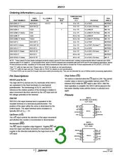
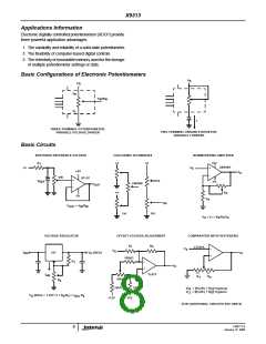
Chip Select (CS)
Pin Descriptions
The device is selected when the CS input is LOW. The current
RH/VH and RL/VL
counter value is stored in nonvolatile memory when CS is
The high (RH/VH) and low (RL/VL) terminals of the X9313
returned HIGH while the INC input is also HIGH. After the
are equivalent to the fixed terminals of a mechanical
store operation is complete, the X9313 will be placed in the
potentiometer. The terminology of RL/VL and RH/VH
low power standby mode until the device is selected once
references the relative position of the terminal in relation to
again.
wiper movement direction selected by the U/D input and not
the voltage potential on the terminal.
Pinouts
X9313
(8 LD PDIP, 8 LD SOIC)
RW/VW
RW/VW is the wiper terminal and is equivalent to the
movable terminal of a mechanical potentiometer. The
position of the wiper within the array is determined by the
control inputs. The wiper terminal series resistance is
TOP VIEW
INC
1
2
3
4
8
7
6
5
VCC
U/D
RH/VH
VSS
CS
typically 40Ω at V
= 5V.
X9313
CC
RL/VL
RW/VW
Up/Down (U/D)
The U/D input controls the direction of the wiper movement
and whether the counter is incremented or decremented.
X9313
(8 LD MSOP)
Increment (INC)
TOP VIEW
The INC input is negative-edge triggered. Toggling INC will
move the wiper and either increment or decrement the
counter in the direction indicated by the logic level on the
U/D input.
RH/VH
U/D
INC
VCC
1
8
7
6
5
VSS
RW/VW
RL/VL
2
3
4
X9313
CS
FN8177.6
January 15, 2008
3

 RENESAS [ RENESAS TECHNOLOGY CORP ]