R8C/13 Group Hardware Manual
REVISION HISTORY
Rev.
Date
Description
Summary
Page
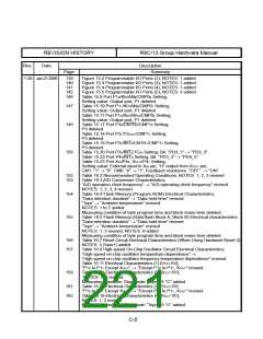
1.20 Jan.27.2006
9
3 Memory, Figure 3.1 Memory Map;
“Program area” → “Program ROM”, “Data area” → “Data flash” revised
Table 4.1 SFR Information(1) NOTES:1 revised
Table 4.2 SFR Information(2) NOTES:1 revised
10
11
12
Table 4.3 SFR Information(3);
008116: “Prescaler Y” → “Prescaler Y Register”
008216: “Timer Y Secondary” → “Timer Y Secondary Register”
008316: “Timer Y Primary” → “Timer Y Primary Register”
008516: “Prescaler Z” → “Prescaler Z Register”
008616: “Timer Z Secondary” → “Timer Z Secondary Register”
008716: “Timer Z Primary” → “Timer Z Primary Register”
008C16: “Prescaler X” → “Prescaler X Register” revised
NOTES:1, 2 revised
13
15
18
29
Table 4.4 SFR Information(4) NOTES:1 revised
Figure 5.2 Reset Sequence; “72cycles” → “64cycles” revised
5.1.3 Power-on Reset Function revised
6 Clock Generation Circuit;
“(oscillation stop detect function)” → “(oscillation stop detection function)” revised
Table 6.1 Clock Generation Circuit Specifications NOTES: 2 deleted
Figure 6.3 OCD Register NOTES: 3 partly deleted
32
35
6.2.1 Low-Speed On-Chip Oscillator Clock;
“The application products ... to accommodate the frequency range.” →
“The application products ... for the frequency change.” revised
Table 6.2 Setting Clock Related Bit and Modes CM13 added
6.5.1 How to Use Oscillation Stop Detection Function:
“This function cannot ... is below 2 MHz.” added
38
42
46
Table 9.1 Bus Cycles for Access Space, Table 9.2 Access Unit and Bus Operation;
“SFR” → “SFR, Data flash”,
ROM/RAM” → “Program ROM/RAM” revised
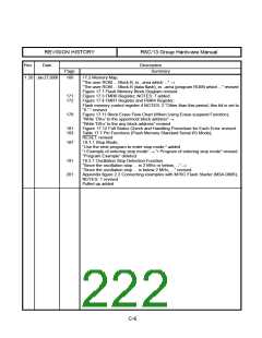
51
59
71
74
88
102
107
108
111
Table 10.2 Relocatable Vector Tables; “A/D” → “A/D Conversion” revised
Figure 10.9 Interrupts Priority Select Circuit NOTES: 1 deleted
Figure 12.1 Timer X Block Diagram; “Peripheral data bus” → “Data bus” revised
Table 12.3 Pulse Output Mode Specifications NOTES: 1 added
Figure 12.18 Timer Z Block Diagram; “Peripheral data bus” → “Data bus” revised
Figure 12.30 CMP Waveform Output Unit revised
Table 12.14 Output Compare Mode Specifications NOTES: 2 revised
Figure 12.34 Operation Example of Timer C in Output Compare Mode revised
Figure 13.3 U0TB to U1TB Registers, U0RB and U1RB Registers, and U0BRG and
U1BRG Registers;
UARTi transmit buffer register (i=0, 1) revised
UARTi bit rate register (i=0, 1); NOTES: 3 added
112
113
120
Figure 13.4 U0MR to U1MR Registers and U0C0 and U1C0 Registers;
UARTi transmit/receive control register 0 (i=0, 1); NOTES: 1 added
Figure 13.5 U0C1 and U1C1 Registers and UCON Register;
UART transmit/receive control register 2; NOTES: 2 added
Table 13.5 Registers to Be Used and Settings in UART Mode;
UiBRG: “–” → “0 to 7” revised
125
135
138
Figure 14.1 A/D Converter Block Diagram “Vref” → “Vcom” revised
14.7 Output Impedance of Sensor under A/D Conversion added
Figure 15.1 Programmable I/O Ports (1); NOTES: 1 added
C-4

 RENESAS [ RENESAS TECHNOLOGY CORP ]