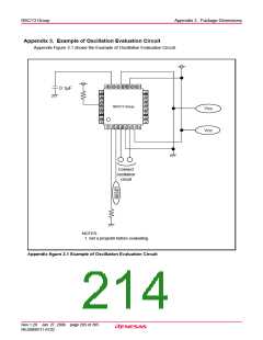
R8C/13 Group
20. Usage Notes for On-chip Debugger
20. Usage notes for on-chip debugger
When using the on-chip debugger to develop the R8C/13 group program and debug, pay the following
attention.
(1) Do not use P00/AN7/TxD11 pin and P37/TxD10/RxD1 pin.
(2) When write in the PD3 register (00E716 address), set bit 7 to "0".
(3) Do not access the related serial interface 1 register.
(4) Do not use from OC00016 address to OC7FF16 address because the on-chip debugger uses these
addresses.
(5) Do not set the address match interrupt (the registers of AIER, RMAD0, RMAD1 and the fixed
vector tables) in a user system.
(6) Do not use the BRK instruction in a user system.
(7) Do not set the b5 to “0” by a user program since the on-chip debugger uses after setting the b5 in
the FMR0 register to “1”.
(8) The stack pointer with up to 8 bytes is used during the user program break. Therefore, save space
of 8 bytes for the stack area.
Connecting and using the on-chip debugger has some peculiar restrictions. Refer to each on-chip
debugger manual for on-chip debugger details.
Rev.1.20 Jan 27, 2006 page 199 of 205
REJ09B0111-0120

 RENESAS [ RENESAS TECHNOLOGY CORP ]