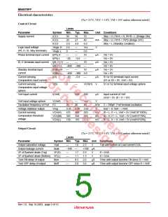
M54679FP
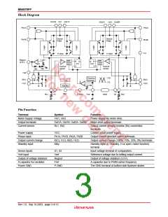
Block Diagram
Out1B Vm1 Out1A
Out2A
Vm2 Out2B
Ph1A
Ph1B
Ph2A
Ph2B
Source
PWM
Source
PWM
V
CC
P.GND
P.GND
1.25V
10K
Regout
(3.5V)
Spike
current
cancel
Spike
current
cancel
R
FF1
S
Q
Q
FF2
R
S
Current
comp1
Current
comp2
18K
Vref
VTH
VTL
Frequency
Generator
I0(1)
I1(1)
I0(2)
I1(2)
TSD
VTM
Standby
Stby
S1
Rs1
P.GND
Fref
GND
S2
RS2
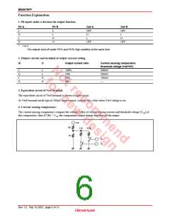
Pin Function
Terminal
Symbol
Function
Motor Supply Voltage
Output terminals
Current sensor
Vm1, Vm2
Power supply for motor drive.
Motor drive output terminals.
Out1A, Out1B, Out2A, Out2B
Rs1, Rs2
Output current sensing resistor (Rs) connection
terminals.
Power supply
VCC
Control circuit power supply.
Phase input
Ph1A, Ph1B, Ph2A, Ph2B
I0(1), I1(1), I0(2), I1(2)
Stby
Output current direction switch terminals.
Output current change
Standby input
Output current change (100%, 70%, 33%, 0%) terminals.
Standby input (L: Standby, H or open: motor function)
terminal.
Sense inputs
Vref input
S1, S2
Vref
Input voltage terminal of comparators.
Reference voltage due to setting output current.
Output of voltage stabilizer (3.5V).
Output of voltage stabilizer
A capacitor for oscillator
Power GND
Regout
Fref
A capacitor due to PWM carrier frequency.
The GND terminal of bottom side flywheel diodes.
P.GND
Rev.1.0, Sep.19.2003, page 3 of 12

 RENESAS [ RENESAS TECHNOLOGY CORP ]