MITSUBISHI MICROCOMPUTERS
M37905F8CFP, M37905F8CSP
16-BIT CMOS MICROCOMPUTER
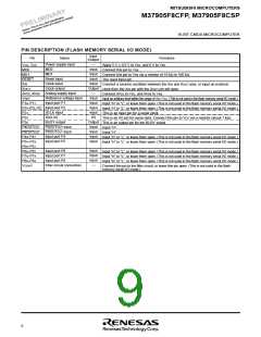
PIN DESCRIPTION (FLASH MEMORY SERIAL I/O MODE)
Input
/Output
Pin
Name
Functions
—
Input
Input
Input
Input
Output
—
Power supply input
MD0
VCC, VSS
MD0
Apply 5 V ± 0.5 V to Vcc, and 0 V to Vss.
Connect this pin to Vss.
MD1
MD1
Connect this pin to Vss via a resistor of 10 kΩ to 100 kΩ.
The reset input pin.
_____
RESET
XIN
Reset input
Clock input
Connect a ceramic oscillator between the XIN and XOUT pins, or input an external
clock from the XIN pin with the XOUT pin left open.
Clock output
Analog supply input
Reference voltage input
Input port P1
Input port P2
SCLK input
XOUT
AVcc, AVss
VREF
Connect AVcc to Vcc, and AVss to Vss.
Input
Input
Input
Input
I/O
Input an arbitrary level within the range of VSS–VCC. (This is not used in the flash memory serial I/O mode.)
Input “H” or “L”, or leave them open. (This is not used in the flash memory serial I/O mode.)
Input “H” or “L”, or leave them open. (This is not used in the flash memory serial I/O mode.)
This is an input pin for a serial clock.
P10–P17
P20–P23, P27
P24
P25
P26
SDA I/O
This is an I/O pin for serial data. Connect this pin to VCC via a resistor (about 1 kΩ).
This is an output pin for the BUSY signal.
Output
Input
Input
Input
Input
BUSY output
P4OUTCUT input
P6OUTCUT input
Input port P4
Input port P5
P4OUTCUT
P6OUTCUT
P40–P47
P55–P53,
P55–P57
P60–P67
P70–P74
P80–P83
VCONT
Input “H”.
Input “H”.
Input “H” or “L”, or leave them open. (This is not used in the flash memory serial I/O mode.)
Input “H” or “L”, or leave them open. (This is not used in the flash memory serial I/O mode.)
Input
Input
Input
—
Input port P6
Input “H” or “L”, or leave them open. (This is not used in the flash memory serial I/O mode.)
Input “H” or “L”, or leave them open. (This is not used in the flash memory serial I/O mode.)
Input “H” or “L”, or leave them open. (This is not used in the flash memory serial I/O mode.)
Input port P7
Input port P8
Filter circuit connection
Connect this pin to the filter circuit, or leave this pin open. (This is not used in the flash
memory serial I/O mode.)
8

 RENESAS [ RENESAS TECHNOLOGY CORP ]