MITSUBISHI MICROCOMPUTERS
M37270MF-XXXSP
M37270EF-XXXSP, M37270EFSP
SINGLE-CHIP 8-BIT CMOS MICROCOMPUTER with CLOSED CAPTION DECODER
and ON-SCREEN DISPLAY CONTROLLER
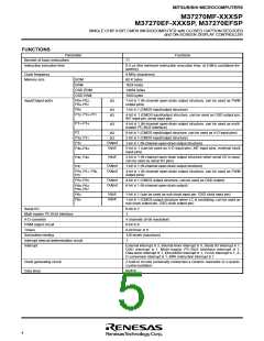
PIN DESCRIPTION
Input/
Output
Pin
Name
Functions
VCC,
Apply voltage of 5 V ± 10 % (typical) to VCC and AVCC, and 0 V to VSS.
Power source
AVCC,
VSS.
CNVSS
RESET
This is connected to VSS.
CNVSS
Input
To enter the reset state, the reset input pin must be kept at a “L” for 2 µs or more (under
normal VCC conditions).
Reset input
If more time is needed for the quartz-crystal oscillator to stabilize, this “L” condition should
be maintained for the required time.
XIN
Input
This chip has an internal clock generating circuit. To control generating frequency, an
external ceramic resonator or a quartz-crystal oscillator is connected between pins XIN and
XOUT. If an external clock is used, the clock source should be connected to the XIN pin and
the XOUT pin should be left open.
Clock input
XOUT
Output
Clock output
P00/PWM4–
P02/PWM6,
P03,
P04/PWM0–
P07/PWM3
I/O
I/O port P0
Port P0 is an 8-bit I/O port with direction register allowing each I/O bit to be individually
programmed as input or output. At reset, this port is set to input mode. The output structure
of P03 is CMOS output, that of P00–P02 and P04–P07 are N-channel open-drain output.
The note out of this Table gives a full of port P0 function.
Output
I/O
Pins P00–P02 and P04–P07 are also used as PWM output pins PWM4–PWM6 and PWM0–
PWM3 respectively. The output structure is N-channel open-drain output.
PWM output
I/O port P1
P10/OUT2,
P11/SCL1,
P12/SCL2,
P13/SDA1,
P14/SDA2,
P15/I1,
Port P1 is an 8-bit I/O port and has basically the same functions as port P0. The output
structure of P10 and P15–P17 is CMOS output, that of P11–P14 is N-channel open-drain
output.
Output
Output
Input
I/O
Pins P10, P15, P16 are also used as OSD output pins OUT2, I1, I2 respectively. The output
structure is CMOS output.
OSD output
Multi-master
Pins P11–P14 are used as SCL1, SCL2, SDA1 and SDA2 respectively, when multi-master
P16/I2/INT3,
P17/SIN
2
2
I C-BUS interface is used. The output structure is N-channel open-drain output.
I C-BUS interface
P17 pin is also used as serial I/O data input pin SIN.
Serial I/O data
input
P20–P23
P24/AD3–
P26/AD1,
P27
Port P2 is an 8-bit I/O port and has basically the same functions as port P0. The output
structure is CMOS output.
I/O port P2
Analog input
I/O port P3
Input
I/O
Pins P24–P26 are also used as analog input pins AD3–AD1 respectively.
P30, P31
Ports P30 and P31 are a 2-bit I/O port and has basically the same functions as port P0. The
output structure is CMOS output.
Output
Input
Input
Input
P32
Port P32 is a 1-bit output port. The output structure is N-channel open-drain output.
Ports P40–P46 are a 7-bit input port.
Output port P3
Input port P4
Analog input
P40/AD4,
P41/INT2,
P42/TIM2,
P43/TIM3,
P44/INT1,
P45/SOUT,
P46/SCLK,
P40 pin is also used as analog input pin AD4.
External interrupt
input
Pins P41, P44 are also used as external interrupt input INT2, INT1.
Input
External clock input
Pins P42 and P43 are also used as external clock input pins TIM2, TIM3 respectively.
Output
Serial I/O data
output
P45 pin is used as serial I/O data output pin SOUT. The output structure is N-channel open-
drain output.
I/O
Serial I/O
synchronizing clock
input/output
P46 pin is used as serial I/O synchronizing clock input/output pin SCLK. The output struc-
ture is N-channel open-drain output.
Output
Output
P47
Output port P4
Port P47 is a 1-bit output port. The output structure is N-channel open-drain output.
P50/PWN7,
P51, P52/R,
P53/G, P54/B,
P55/OUT1,
P56, P57
Output port P5
Ports P50–P57 are an 8-bit output port. The output structure of P50, P51, P56, P57 are N-
channel open-drain output, that of P52–P55 is CMOS output.
Output
Output
PWM output
OSD output
P50 pin is also used as PWM output pin PWM7.
Pins P52–P55 are also used as OSD output pins R, G, B, OUT1 respectively.
6

 RENESAS [ RENESAS TECHNOLOGY CORP ]