MITSUBISHI MICROCOMPUTERS
M37270MF-XXXSP
M37270EF-XXXSP, M37270EFSP
SINGLE-CHIP 8-BIT CMOS MICROCOMPUTER with CLOSED CAPTION DECODER
and ON-SCREEN DISPLAY CONTROLLER
(5) Timer 5
Timer 5 can select one of the following count sources:
TIMERS
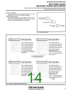
The M37270MF-XXXSP has 6 timers: timer 1, timer 2, timer 3,
f(XIN)/16 or f(XCIN)/16
timer 4, timer 5, and timer 6. All timers are 8-bit timers with the 8-bit
timer latch. The timer block diagram is shown in Figure 8.
All of the timers count down and their divide ratio is 1/(n+1), where n
is the value of timer latch. The value is set to a timer at the same time
by writing a count value to the corresponding timer latch (addresses
00F016 to 00F316 : timers 1 to 4, addresses 020C16 and 020D16 :
timers 5 and 6).
•
Timer 2 overflow signal
•
Timer 4 overflow signal
•
The count source of timer 3 is selected by setting bit 6 of the timer
mode register 1 (address 00F416) and bit 7 of the timer mode regis-
ter 2 (address 00F516). Either f(XIN) or f(XCIN) is selected by bit 7 of
the CPU mode register.
Timer 5 interrupt request occurs at timer 5 overflow.
The count value is decremented by 1. The timer interrupt request bit
is set to “1” by a timer overflow at the next count pulse after the count
value reaches “0016”.
(6) Timer 6
Timer 6 can select one of the following count sources:
f(XIN)/16 or f(XCIN)/16
•
•
(1) Timer 1
Timer 5 overflow signal
Timer 1 can select one of the following count sources:
The count source of timer 6 is selected by setting bit 7 of the timer
mode register 1 (address 00F416). Either f(XIN) or f(XCIN) is selected
by bit 7 of the CPU mode register. When timer 5 overflow signal is a
count source for the timer 6, the timer 5 functions as an 8-bit prescaler.
Timer 6 interrupt request occurs at timer 6 overflow.
f(XIN)/16 or f(XCIN)/16
•
f(XIN)/4096 or f(XCIN)/4096
•
External clock from the P42/TIM2 pin
•
The count source of timer 1 is selected by setting bits 5 and 0 of the
timer mode register 1 (address 00F416). Either f(XIN) or f(XCIN) is
selected by bit 7 of the CPU mode register.
At reset, timers 3 and 4 are connected by hardware and “FF16” is
Timer 1 interrupt request occurs at timer 1 overflow.
✽
automatically set in timer 3; “0716” in timer 4. The f(XIN) /16 is se-
lected as the timer 3 count source. The internal reset is released by
timer 4 overflow at these state, the internal clock is connected.
At execution of the STP instruction, timers 3 and 4 are connected by
hardware and “FF16” is automatically set in timer 3; “0716” in timer 4.
(2) Timer 2
Timer 2 can select one of the following count sources:
f(XIN)/16 or f(XCIN)/16
•
Timer 1 overflow signal
•
✽
However, the f(XIN) /16 is not selected as the timer 3 count source.
External clock from the P42/TIM2 pin
•
So set both bit 0 of the timer mode register 2 (address 00F516) and
bit 6 at address 00C716 to “0” before the execution of the STP in-
The count source of timer 2 is selected by setting bits 4 and 1 of the
timer mode register 1 (address 00F416). Either f(XIN) or f(XCIN) is
selected by bit 7 of the CPU mode register. When timer 1 overflow
signal is a count source for the timer 2, the timer 1 functions as an 8-
bit prescaler.
✽
struction (f(XIN) /16 is selected as the timer 3 count source). The
internal STP state is released by timer 4 overflow at these state, the
internal clock is connected.
Because of this, the program starts with the stable clock.
✽ : When bit 7 of the CPU mode register (CM7) is “1,” f(XIN) be-
comes f(XCIN).
Timer 2 interrupt request occurs at timer 2 overflow.
(3) Timer 3
Timer 3 can select one of the following count sources:
The structure of timer-related registers is shown in Figure 7.
f(XIN)/16 or f(XCIN)/16
•
f(XCIN)
•
External clock from the P43/TIM3 pin
•
The count source of timer 3 is selected by setting bit 0 of the timer
mode register 2 (address 00F516) and bit 6 at address 00C716. Ei-
ther f(XIN) or f(XCIN) is selected by bit 7 of the CPU mode register.
Timer 3 interrupt request occurs at timer 3 overflow.
(4) Timer 4
Timer 4 can select one of the following count sources:
f(XIN)/16 or f(XCIN)/16
•
f(XIN)/2 or f(XCIN)/2
•
f(XCIN)
•
The count source of timer 3 is selected by setting bits 4 and 1 of the
timer mode register 2 (address 00F516). Either f(XIN) or f(XCIN) is
selected by bit 7 of the CPU mode register. When timer 3 overflow
signal is a count source for the timer 4, the timer 3 functions as an 8-
bit prescaler.
Timer 4 interrupt request occurs at timer 4 overflow.
14

 RENESAS [ RENESAS TECHNOLOGY CORP ]