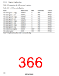
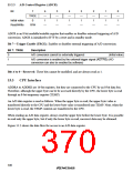
15.2.3
A/D Control Register (ADCR)
Bit
7
TRGE
0
6
—
1
5
—
1
4
—
1
3
—
1
2
—
1
1
—
1
0
—
1
Initial value
Read/Write
R/W
—
—
—
—
—
—
—
ADCR is an 8-bit readable/writable register that enables or disables external triggering of A/D
conversion. ADCR is initialized to H'7F by a reset and in standby mode.
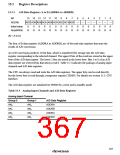
Bit 7—Trigger Enable (TRGE): Enables or disables external triggering of A/D conversion.
Bit 7: TRGE
Description
0
1
A/D conversion cannot be externally triggered
(Initial value)
A/D conversion is enabled by the external trigger signal (ADTRG) (A/D
conversion can also be enabled by software)
Bits 6 to 0—Reserved: These bits cannot be modified, and are always read as 1.
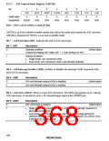
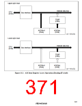
15.3
CPU Interface
ADDRA to ADDRD are 16-bit registers, but they are connected to the CPU by an 8-bit data bus.
Therefore, although the upper byte can be be accessed directly by the CPU, the lower byte is read
through an 8-bit temporary register (TEMP).
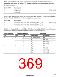
An A/D data register is read as follows. When the upper byte is read, the upper-byte value is
transferred directly to the CPU and the lower-byte value is transferred into TEMP. Next, when the
lower byte is read, the TEMP contents are transferred to the CPU.
When reading an A/D data register, always read the upper byte before the lower byte. It is possible
to read only the upper byte, but if only the lower byte is read, incorrect data may be obtained.
Figure 15.2 shows the data flow for access to an A/D data register.
340

 RENESAS [ RENESAS TECHNOLOGY CORP ]