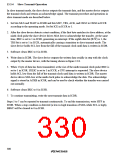
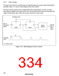
13.3.7
Noise Canceler
The logic levels at the SCL and SDA pins are routed through noise cancelers before being latched
internally. Figure 13.11 shows a block diagram of the noise canceler.
The noise canceler consists of two cascaded latches and a match detector. The SCL (or SDA)
input signal is sampled on the system clock, but is not passed forward to the next circuit unless the
outputs of both latches agree. If they do not agree, the previous value is held.
Sampling clock
C
C
SCL or
SDA input
signal
Internal
SCL or
SDA
D
Q
D
Q
Match
detector
Latch
Latch
signal
t
Sampling
clock
t: System clock
Figure 13.11 Block Diagram of Noise Canceler
304

 RENESAS [ RENESAS TECHNOLOGY CORP ]