Section 18 A/D Converter
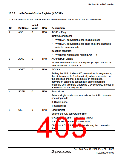
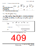
Table 18.3 A/D Conversion Time (Single Mode)
CKS = 0
Typ.
—
CKS = 1
Item
Symbol
Min.
6
Max.
9
Min.
4
Typ.
—
Max.
5
A/D conversion start delay time tD
Input sampling time
A/D conversion time
tSPL
tCONV
—
31
—
—
15
—
131
—
134
69
—
70
Note: All values represent the number of states.
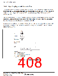
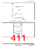
18.4.4
External Trigger Input Timing
A/D conversion can also be started by an external trigger input. When the TRGE bit in ADCR is
set to 1, external trigger input is enabled at the ADTRG pin. A falling edge at the ADTRG input
pin sets the ADST bit in ADCSR to 1, starting A/D conversion. Other operations, in both single
and scan modes, are the same as when the bit ADST has been set to 1 by software. Figure 18.3
shows the timing.
φ
ADTRG
Internal trigger signal
ADST
A/D conversion
Figure 18.3 External Trigger Input Timing
Rev. 3.00 Sep. 10, 2007 Page 375 of 528
REJ09B0216-0300

 RENESAS [ RENESAS TECHNOLOGY CORP ]