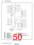
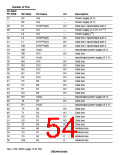
1.2
Block Diagram
SH-3
CPU
MMU
TLB
UBC
AUD
CCN
SCI
CACHE
TMU
RTC
BRIDGE
BSC
UDI
INTC
IrDA
SCIF
ADC
DAC
DMAC
CMT
CPG/WDT
I/O port
External bus
interface
Legend:
ADC:
AUD:
BSC:
CACHE:
CCN:
CMT:
A/D converter
INTC:
IrDA:
MMU:
RTC:
SCI:
Interrupt controller
Advanced user debugger
Bus state controller
Cache memory
Cache memory controller
Compare match timer
Serial communicatiion interface (with IrDA)
Memory management unit
Realtime clock
Serial communication interface (with smart card interface)
Serial communication interface (with FIFO)
Address translation buffer
SCIF:
TLB:
CPG/WDT: Clock pulse generator/watchdog timer
CPU:
DAC:
DMAC:
UDI:
Central processing unit
D/A converter
Direct memory access controller
User debugging interface
TMU:
UBC:
Timer unit
User break controller
Figure 1.1 Block Diagram
Rev. 5.00, 09/03, page 6 of 760

 RENESAS [ RENESAS TECHNOLOGY CORP ]