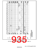
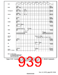
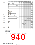
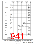
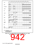
Td3
Td4
Tr
Trw
Tc1
Tc2
Tc3
Tc4/Td1
Td2
CKIO
tAD
tAD
BANK
Row
tAD
tRWD
Precharge-sel
Address
Row
H/L
tRWD
Row
c0
tCSD
tCSD
tRWD
tRWD
RD/
tRASD
tRASD
tCASD2 tCASD2
tCASD2
tDQMD
tDQMD
DQMn
tRDS
tRDH
D63–D0
(read)
d0
d1
d2
d3
tWDD
tWDD
D63–D0
(write)
tBSD
tBSD
tDACD
tDACD
tDACD
DACKn
(SA: IO ← memory)
Notes: IO: DACK device
SA: Single address DMA transfer
DA: Dual address DMA transfer
DACK set to active-high
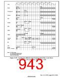
Figure 22.25 Synchronous DRAM Normal Read Bus Cycle: ACT + READ Commands,
Burst (RCD[1:0] = 01, CAS Latency = 3)
Rev. 6.0, 07/02, page 887 of 986

 RENESAS [ RENESAS TECHNOLOGY CORP ]