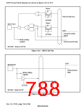
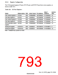
Table 18.2 shows the SCI I/O port pin configuration.
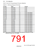
Table 18.2 SCI I/O Port Pins
Pin Name
Abbreviation
MD0/SCK
RxD
I/O
Function
Serial clock pin
Receive data pin
Transmit data pin
I/O
Clock input/output
Receive data input
Transmit data output
Input
Output
MD7/TxD
Note: Pins MD0/SCK and MD7/TxD function as mode input pins MD0 and MD7 after a power-on
reset. They are made to function as serial pins by performing SCI operation settings with
the TE, RE, CKEI, and CKE0 bits in SCSCR1 and the C/$ bit in SCSMR1. Break state
transmission and detection can be performed by means of a setting in the SCI’s SCSPTR1
register.
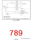
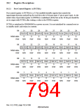
Table 18.3 shows the SCIF I/O port pin configuration.
Table 18.3 SCIF I/O Port Pins
Pin Name
Abbreviation
05(6(7/SCK2
MD2/RxD2
MD1/TxD2
&765
I/O
Function
Serial clock pin
Receive data pin
Transmit data pin
Modem control pin
Modem control pin
Input
Input
Output
I/O
Clock input
Receive data input
Transmit data output
Transmission enabled
Transmission request
MD8/5765
I/O
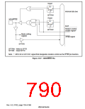
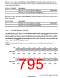
Note: The MRESET/SCK2 pin functions as the 05(6(7 manual reset pin when a manual reset is
executed. The MD1/TxD2, MD2/RxD2, and MD8/5765 pins function as the MD1, MD2, and
MD8 mode input pins after a power-on reset. These pins are made to function as serial pins
by performing SCIF operation settings with the TE and RE bits in SCSCR2 and the MCE bit
in SCFCR2. Break state transmission and detection can be set in the SCIF’s SCSPTR2
register.
Rev. 6.0, 07/02, page 740 of 986

 RENESAS [ RENESAS TECHNOLOGY CORP ]