13.3.10 Waits between Access Cycles
A problem associated with higher external memory bus operating frequencies is that data buffer
turn-off on completion of a read from a low-speed device may be too slow, causing a collision
with the data in the next access, and so resulting in lower reliability or incorrect operation. To
avoid this problem, a data collision prevention feature has been provided. This memorizes the
preceding access area and the kind of read/write, and if there is a possibility of a bus collision
when the next access is started, inserts a wait cycle before the access cycle to prevent a data
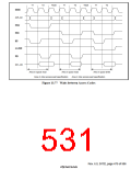
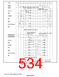
collision. Wait cycle insertion consists of inserting idle cycles between access cycles, as shown in
section 13.2.5, Wait Control Register (WCR1). When the SH7750 Series performs consecutive
write cycles, the data transfer direction is fixed (from the SH7750 Series to other memory) and
there is no problem. With read accesses to the same area, also, in principle data is output from the
same data buffer, and wait cycle insertion is not performed. If there is originally space between
accesses, according to the setting of bits AnIW2–AnIW0 (n = 0 to 6) in WCR1, the number of idle
cycles inserted is the specified number of idle cycles minus the number of empty cycles.
When bus arbitration is performed, the bus is released after waits are inserted between cycles.
In single address mode DMA transfer, when data transfer is performed from an I/O device to
memory the data on the bus is determined by the speed of the I/O device. With a low-speed I/O
device, an inter-cycle idle wait equivalent to the output buffer turn-off time must be inserted. Even
with high-speed memory, when DMA transfer is considered, it may be necessary to insert an inter-
cycle wait to adjust to the speed of a low-speed device, preventing the memory from being used at
full speed.
Bits DMAIW2–DMAIW0 in wait control register 1 (WCR1) allow an inter-cycle wait setting to
be made when transferring data from an I/O device to memory using single address mode DMA
transfer. From 0 to 15 waits can be inserted. The number of waits specified by DMAIW2–
DMAIW0 are inserted in single address DMA transfers to all areas.
In dual address mode DMA transfer, the normal inter-cycle wait specified by AnIW2–AnIW0 (n =
0 to 6) is inserted.
Rev. 6.0, 07/02, page 478 of 986

 RENESAS [ RENESAS TECHNOLOGY CORP ]