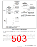
13.3.8 MPX Interface
If the MD6 pin is set to 0 in a power-on reset by the 5(6(7 pin, the MPX interface for normal
memory is selected for area 0. The MPX interface is selected for areas 1 to 6 by means of the
MPX bit in BCR1 and the MEMMODE, A4MPX, and AIMPX bits in BCR3. The MPX interface
offers a multiplexed address/data type bus protocol, and permits easy connection to an external
memory controller chip that uses a single 32-bit multiplexed address/data bus. A bus cycle
consists of an address phase and a data phase. In the address phase, the address information is
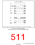
output to D25−D0, and the access size to D63−D61 and D31–D29*.
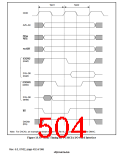
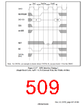
The %6 signal which indicates the address phase is asserted for one cycle. The &6Q signal is
asserted at the rise of Tm1, and negated after the last data transfer in the data phase. Therefore, a
negate period does not exist for access with the minimum pitch. The )5$0( signal is asserted at
the rise of Tm1, and negated when the cycle of the last data transfer starts in the data phase.
Therefore, in an external device supporting the MPX interface, the address information and access
size output in the address phase must be saved in the external device memory, and data
corresponding to the data phase must be input or output.
For details of access sizes and data alignment, see section 13.3.1, Endian/Access Size and Data
Alignment.
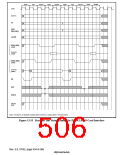
The address pins output at A25–A0 are undefined.
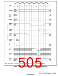
32-byte transfer performed consecutively for a total of 32 bytes according to the set bus width.
The first access is performed on the data for which there was an access request, and the remaining
accesses are performed on the data at the 32-byte boundary. When the access size is larger than the
data bus width, as in this case, burst access is generated, with the address output once, followed by
multiple data cycles. The bus is not released during this period.
Note: * SH7750R only.
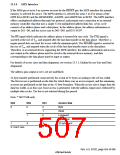
D63
D62
D61
0
Access Size
Byte
0
0
1
Word
1
0
Longword
Quadword
32-byte burst
1
1
X
X
X: Don’t care
Rev. 6.0, 07/02, page 455 of 986

 RENESAS [ RENESAS TECHNOLOGY CORP ]