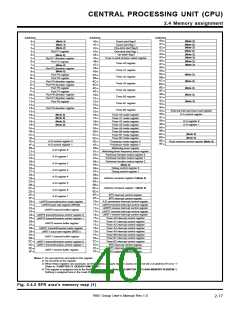
CENTRAL PROCESSING UNIT (CPU)
2.2 Bus interface unit (BIU)
(a) When accessing 8-bit data (Note 1) or accessing 16-bit data starting from an even-numbered address
φBIU
Internal address bus
Address
(AD0–AD23)
Note 1: When reading 8-bit data at an even-numbered address, only RD (even)
RD
(even)
will be taken into a data buffer.
When reading 8-bit data at an odd-numbered address, only RD (odd)
will be taken into a data buffer.
When writing 8-bit data to an even-numbered address, only WD (even)
will be written to the address.
Internal data bus
(DB0–DB7)
WD (even)
RD
(odd)
When writing 8-bit data to an odd-numbered address, only WD (odd)
will be written to the address.
Internal data bus
(DB8–DB15)
WD (odd)
(b) When accessing 16-bit data starting from an odd-numbered address
φBIU
Internal address bus
Address
Address + 1
(AD0–AD23)
RD
(even)
Internal data bus
(DB0–DB7)
WD (even)
RD
(odd)
Internal data bus
(DB8–DB15)
WD (odd)
(c) When accessing 32-bit data starting from an even-numbered address
φBIU
Internal address bus
Address
Address + 2
(AD0–AD23)
RD
RD
(even)
(even)
Internal data bus
(DB0–DB7)
WD (even)
WD (even)
RD
(odd)
RD
(odd)
Internal data bus
(DB8–DB15)
WD (odd)
WD(odd)
(d) When accessing 32-bit data starting from an odd-numbered address
φBIU
Internal address bus
Address
Address + 1
Address + 3
(AD0–AD23)
RD
RD
(even)
(even)
Internal data bus
(DB0–DB7)
WD (even)
WD (even)
RD
RD
(odd)
(odd)
Internal data bus
(DB8–DB15)
WD (odd)
WD (odd)
RD: Data to be read, WD: Data to be written
Note 2: The above waveforms apply when bus cycle = 2φ.
For the bus cycles at access to the internal area, see Table 2.2.4.
Fig. 2.2.4 Operation waveform examples at reading from or writing to internal area
7905 Group User’s Manual Rev.1.0
2-13

 RENESAS [ RENESAS TECHNOLOGY CORP ]