SERIAL I/O
11.4 Clock asynchronous serial I/O (UART) mode
11.4 Clock asynchronous serial I/O (UART) mode
Table 11.4.1 lists the performance overview in the UART mode, and Table 11.4.2 lists the functions of
I/O pins in this mode.
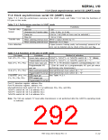
Table 11.4.1 Performance overview in UART mode
Item
Functions
Transfer data
format
1 bit
Start bit
7 bits, 8 bits, or 9 bits
Character bit (Transfer data)
Parity bit
0 bit or 1 bit (Odd or Even can be selected.)
1 bit or 2 bits
Stop bit
Transfer rate
BRGi’s output divided by 16
When selecting internal clock
When selecting external clock
Maximum 312.5 kbps
Error detection
4 types (overrun, framing, parity, and summing): presence of an
error can be detected only by check of the error sum flag.
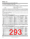
Table 11.4.2 Functions of I/O pins in UART mode
Method of selection
Pin name
(P1 , P1 , P8 )
Functions
Serial data output pin
Programmable I/O port pin
Serial data input pin
Programmable I/O
port pin
TxD
TxD
0
0
/P1
/P1
3
3
, TxD
, TxD
1
1
/P1
/P1
7
7
, or TxD
, or TxD
2
/P8
/P8
3
switch bit = “0.” (Note)
TxD
i
3
7
3
2
3
switch bit = “1.”
Port P1 or P8 direction register’s corresponding bit = “0”
– (Can be used as a programmable I/O port pin when
performing only transmission.)
RxD
CLK
i
i
(P1
(P1
2
1
, P1
, P1
6
, P8
, P8
2
)
)
Internal/External clock select bit = “1”
Internal/External clock select bit = “0”
See Table 11.2.1.
5
1
BRGi’s count source input pin
Programmable I/O port pin
, CTS input pin
CTSi/RTSi (P1
0
, P1
1
P1
4
, P1
5
, P8
0
, P8
1
)
RTS output pin
Programmable I/O port pin
Port P1 direction register: address 0516
Port P8 direction register: address 1416
Internal/External clock select bit: bit 3 at addresses 3016, 3816, and B016
TxD
TxD
TxD
0
1
2
/P1
/P1
/P8
3
7
3
switch bit: bit 2 at address AC16
switch bit: bit 3 at address AC16
switch bit: bit 5 at address AC16
Note: The TxD
i
pin outputs “H” level while transmission is not performed after the UARTi’s operating mode
is selected.
7905 Group User’s Manual Rev.1.0
11-37

 RENESAS [ RENESAS TECHNOLOGY CORP ]