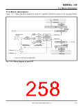
SERIAL I/O
11.2 Block description
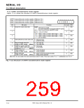
11.2.2 UARTi transmit/receive control register 0
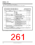
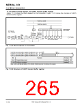
Figure 11.2.3 shows the structure of UARTi transmit/receive control register 0.
UART0 transmit/receive control register (Address 3416
UART1 transmit/receive control register (Address 3C16
UART2 transmit/receive control register (Address B416
)
)
)
b7 b6 b5 b4 b3 b2 b1 b0
At reset R/W
Function
Bit
0
Bit name
b1 b0
0
0
0
1
RW
RW
RW
RO
BRG count source select bits
0 0 : Clock f2
0 1 : Clock f16
1 0 : Clock f64
1 1 : Clock f512
1
2
3
0 : The CTS function is selected.
1 : The RTS function is selected.
CTS/RTS function select bit
(Note 1)
Transmit register empty flag
0 : Data is present in the transmit register.
(Transmission is in progress.)
1 : No data is present in the transmit register.
(Transmission is completed.)
0
0
0
RW
RW
RW
0 : The CTS/RTS function is enabled.
1 : The CTS/RTS function is disabled.
4
5
6
CTS/RTS enable bit
0 : Reception interrupt
1 : Reception error interrupt
UARTi receive interrupt mode
select bit
CLK polarity select bit
(This bit is used in the clock
synchronous serial I/O mode.)
(Note 2)
0 : At the falling edge of the transfer clock, transmit
data is output; at the rising edge of the transfer
clock, receive data is input.
When not in transferring, pin CLKi’s level is “H.”
1 : At the falling edge of the transfer clock, transmit
data is output; at the falling edge of the transfer
clock, receive data is input.
When not in transferring, pin CLKi’s level is “L.”
0
RW
0 : LSB (Least Significant Bit) first
1 : MSB (Most Significant Bit) first
Transfer format select bit
(This bit is used in the clock
synchronous serial I/O mode.)
(Note 2)
7
Notes 1: Valid when the CTS/RTS enable bit (bit 4) is “0” and CTSi/RTSi separate select bit (bit 0, 1, or 4 at address AC16) is “0.”
2: Fix these bits to “0” in the UART mode or when serial I/O is disabled.
Fig. 11.2.3 Structure of UARTi transmit/receive control register 0
7905 Group User’s Manual Rev.1.0
11-6

 RENESAS [ RENESAS TECHNOLOGY CORP ]