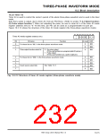
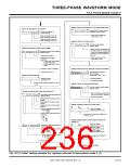
THREE-PHASE WAVEFORM MODE
10.3 Three-phase mode 0
Setting of timers A0 through A2 to one-shot pulse mode
Timers A0 through A3 are inactive.
b7
b0
Timer A0/A1/A2 mode register
b7
b0
0
1
1
0
1
0
Count start register 0
(address 4016
(addresses 5616 to 5816
)
0
0
0
0
)
Count source select bits
(See Table 7.2.3.)
Stops counting in timer A0.
Stops counting in timer A1.
Stops counting in timer A2.
Stops counting in timer A3.
Setting of timer A3 to timer mode
b7
b0
Timer A3 mode register
0
0
0
0
0
(address 5916
)
Setting of waveform output mode register
When not using the TA3OUT pin
(in other words, the TA3OUT pin
is used as a programmable I/O
port pin.), be sure to clear this
bit to “0.”
b7
b0
Waveform output mode register
0
➀ 0 ➀ 1
0
0
(address A616
)
Three-phase mode 0
Count source select bits
(See Table 7.2.3.)
Dead-time timer trigger
select bit
0 : Falling and Rising edges
of one-shot pulse
1 : Falling edge of one-shot
pulse
Waveform outout is disabled.
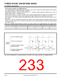
Setting of timer A0/A1/A2 interrupt request to “disabled”
b7
b0
➀ : It may be either “0” or “1.”
Timer A0/A1/A2 interrupt
control register
0
0
0
0
Setting of dead-time timer
(addresses 7516 to 7716
)
b7
b0
Interrupt disabled
Dead-time timer
(address A716
)
No Interrupt request
A value in the range from “0016” to “FF16
is set.
”
Setting of timer A3 interrupt priority level
b7
b0
Timer A3 interrupt control register
0
(address 7816
)
Setting of three-phase output data register 0, 1
Timer A3 interrupt priority level
Set to one of levels 1 through 7.
b7
b0
Three-phase output data register 0
➀ ➀
0
0
0
(address A816
)
No Interrupt request
Released from W-phase output
fixation.
Released from V-phase output
fixation.
Setting of period of timer A3’s carrier wave
Released from U-phase output
fixation.
(b15)
b7
(b8)
b0 b7
b0
W-phase output polarity set buffer
0 : “H” output
1 : “L” output
Timer A3 register
(addresses 4D16, 4C16
)
Clock-source-of-dead-time-timer
select bits
A value in the range from “000016” to
“FFFF16” is set.
b7 b6
0 0 : f
0 1 : f
1 0 : f
2
2
2
/2
/4
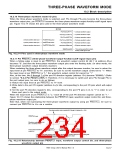
Setting of output width of each phase of timers A0
through A2
b7
b0
(b15)
b7
(b8)
b0 b7
Timer A0 register
(addresses 4716, 4616
Timer A1 register
Three-phase output data register 1
b0
)
)
➀ ➀
➀ ➀ ➀ ➀
(address A916
)
V-phase output polarity set buffer
0 : “H” output
(addresses 4916, 4816
Timer A2 register
1 : “L” output
(addresses 4B16, 4A16)
U-phase output polarity set buffer
0 : “H” output
1 : “L” output
A value in the range from “000016” to
“FFFF16” is set.
➀ : It may be either “0” or “1.”
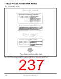
Continues to the next page.
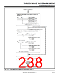
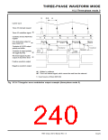
Fig. 10.3.1 Initial setting example for registers relevant to three-phase mode 0 (1)
7905 Group User’s Manual Rev.1.0
10-19

 RENESAS [ RENESAS TECHNOLOGY CORP ]