INTERRUPTS
6.10 External interrupts
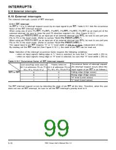
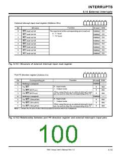
b7 b6 b5 b4 b3 b2 b1 b0
External interrupt input read register (Address 9516
)
Function
Bit
0
Bit name
INT0 read out bit
At reset R/W
The input level at the corresponding pin is read out.
Undefined RO
Undefined RO
Undefined RO
Undefined RO
Undefined RO
Undefined RO
Undefined RO
Undefined RO
0 : “L” level
1 : “H” level
1
INT1 read out bit
INT2 read out bit
INT3 read out bit
INT4 read out bit
INT5 read out bit
INT6 read out bit
INT7 read out bit
2
3
4
5
6
7
Fig. 6.10.1 Structure of external interrupt input read register
b7 b6 b5 b4 b3 b2 b1 b0
Port P5 direction register (Address D16)
Bit
0
Corresponding pin
Nothing is assigned.
Function
At reset R/W
Undefined
—
0 : Input mode
0
1
Pin INT1
RW
RW
RW
—
1 : Output mode
0
2
Pin INT2 (RTPTRG1)
Pin INT3 (RTPTRG0)
Nothing is assigned.
Pin INT5 (TB0IN/IDW)
Pin INT6 (TB1IN/IDV)
Pin INT7 (TB2IN/IDU)
When using this pin as an external interrupt’s input
pin, be sure to clear the corresponding bit to “0.”
0
3
Undefined
4
0 : Input mode
0
0
0
5
RW
RW
RW
1 : Output mode
6
When using this pin as an external interrupt’s input
pin, be sure to clear the corresponding bit to “0.”
7
Note: ( ) shows the I/O pins of other internal peripheral devices which are multiplexed.
Fig. 6.10.2 Relationship between port P5 direction register and external interrupt’s input pins
7905 Group User’s Manual Rev.1.0
6-19

 RENESAS [ RENESAS TECHNOLOGY CORP ]