2SC3356
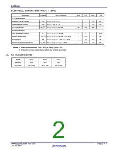
ELECTRICAL CHARACTERISTICS (TA = +25°C)
Parameter
DC Characteristics
Symbol
Test Conditions
MIN.
TYP.
MAX.
Unit
Collector Cut-off Current
Emitter Cut-off Current
DC Current Gain
ICBO
IEBO
VCB = 10 V, IE = 0
–
–
–
–
1.0
1.0
μA
μA
–
VEB = 1.0 V, IC = 0
Note 1
hFE
VCE = 10 V, IC = 20 mA
50
120
250
RF Characteristics
Gain Bandwidth Product
Insertion Power Gain
Noise Figure
fT
VCE = 10 V, IC = 20 mA
–
–
–
−
7
–
GHz
dB
⏐S21e⏐2 VCE = 10 V, IC = 20 mA, f = 1 GHz
11.5
1.1
–
NF
VCE = 10 V, IC = 7 mA, f = 1 GHz
VCB = 10 V, IE = 0, f = 1 MHz
2.0
1.0
dB
Note 2
Reverse Transfer Capacitance
Cre
0.55
pF
Notes 1. Pulse measurement: PW ≤ 350 μs, Duty Cycle ≤ 2%
2. Collector to base capacitance when the emitter grounded
<R>
hFE CLASSIFICATION
Rank
Q/YQ
R23
R/YR
R24
S/YS
R25
Marking
hFE Value
50 to 100
80 to 160
125 to 250
R09DS0021EJ0300 Rev.3.00
Jun 28, 2011
Page 2 of 7

 RENESAS [ RENESAS TECHNOLOGY CORP ]