FM25CL64
Notes
AC Parameters (TA = -40° C to + 85° C, CL = 30pF)
VDD 2.7 to 3.0V
VDD 3.0 to 3.65V
Symbol
fCK
tCH
Parameter
Min
0
25
25
10
10
Max
18
Min
0
Max
20
Units
MHz
ns
ns
ns
ns
ns
ns
ns
SCK Clock Frequency
Clock High Time
Clock Low Time
Chip Select Setup
Chip Select Hold
Output Disable Time
Output Data Valid Time
Output Hold Time
Deselect Time
22
22
10
10
1
1
tCL
tCSU
tCSH
tOD
tODV
tOH
tD
20
25
20
20
2
0
60
0
60
ns
tR
tF
tSU
tH
Data In Rise Time
Data In Fall Time
Data Setup Time
Data Hold Time
50
50
50
50
ns
ns
ns
ns
1,3
1,3
5
5
5
5
tHS
tHH
tHZ
/Hold Setup Time
/Hold Hold Time
/Hold Low to Hi-Z
/Hold High to Data Active
10
10
10
10
ns
ns
ns
ns
20
20
20
20
2
2
tLZ
Notes
1. tCH + tCL = 1/fCK
.
2. Characterized but not 100% tested in production.
3. Rise and fall times measured between 10% and 90% of waveform.
Capacitance (TA = 25° C, f=1.0 MHz, VDD = 3.3V)
Symbol
CO
CI
Parameter
Output capacitance (SO)
Input capacitance
Min
-
-
Max
8
6
Units
pF
pF
Notes
1
1
Notes
1. This parameter is periodically sampled and not 100% tested.
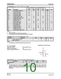
Equivalent AC Load Circuit
AC Test Conditions
Input Pulse Levels
Input rise and fall times
Input and output timing levels
10% and 90% of VDD
5 ns
30% and 70% of VDD
3.3V
1.2K Ω
Output
0.95K Ω
30 pF
Data Retention (VDD = 2.7V to 3.65V unless otherwise specified)
Parameter
Data Retention
Notes
Min
10
Max
-
Units
Years
Notes
1
1. The relationship between retention, temperature, and the associated reliability level is characterized
separately. Endurance is the guaranteed number of read or write cycles per address that can be
performed while maintaining the specified data retention. It is unlikely to reach this limit for most
applications.
Rev. 2.1
Apr. 2003
Page 10 of 13

 RAMTRON [ RAMTRON INTERNATIONAL CORPORATION ]