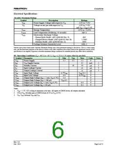
FM18W08
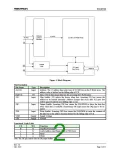
Address
Latch &
Decoder
A(14:0)
A(14:0)
32,768 x 8 FRAM Array
CE
Control
Logic
WE
OE
I/O Latch
Bus Driver
DQ(7:0)
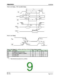
Figure 1. Block Diagram
Pin Description
Pin Name
Type
Description
A(14:0)
Input
Address: The 15 address lines select one of 32,768 bytes in the F-RAM array. The
address value is latched on the falling edge of /CE.
DQ(7:0)
/CE
I/O
Input
Data: 8-bit bi-directional data bus for accessing the F-RAM array.
Chip Enable: /CE selects the device when low. Asserting /CE low causes the
address to be latched internally. Address changes that occur after /CE goes low
will be ignored until the next falling edge occurs.
/OE
Input
Input
Output Enable: Asserting /OE low causes the FM18W08 to drive the data bus
when valid data is available. Deasserting /OE high causes the DQ pins to be tri-
stated.
Write Enable: Asserting /WE low causes the FM18W08 to write the contents of
the data bus to the address location latched by the falling edge of /CE.
Supply Voltage
/WE
VDD
VSS
Supply
Supply
Ground
Functional Truth Table
/CE
H
L
L
/WE
Function
Standby/Precharge
Latch Address (and Begin Write if /WE=low)
Read
X
X
H
Write
Note: The /OE pin controls only the DQ output buffers.
Rev. 2.0
Dec. 2011
Page 2 of 11

 RAMTRON [ RAMTRON INTERNATIONAL CORPORATION ]