FM18W08
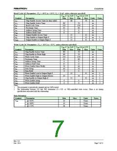
Read Cycle AC Parameters (TA = -40C to + 85C, CL = 30 pF, unless otherwise specified)
VDD 2.7 to 3.0V VDD 3.0 to 5.5V
Symbol
tCE
tCA
tRC
tPC
tAS
tAH
tOE
tHZ
Parameter
Min
Max
80
Min
Max Units Notes
Chip Enable Access Time (to data valid)
Chip Enable Active Time
Read Cycle Time
Precharge Time
Address Setup Time
70
ns
ns
ns
ns
ns
ns
ns
ns
ns
80
145
65
0
70
130
60
0
Address Hold Time
15
15
Output Enable Access Time
Chip Enable to Output High-Z
Output Enable to Output High-Z
15
15
15
12
15
15
1
1
tOHZ
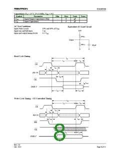
Write Cycle AC Parameters (TA = -40C to + 85C, unless otherwise specified)
VDD 2.7 to 3.0V VDD 3.0 to 5.5V
Symbol
tCA
tCW
tWC
tPC
tAS
tAH
tWP
tDS
tDH
Parameter
Min
80
80
145
65
0
15
50
40
0
Max
Min
70
70
130
60
0
15
40
30
0
Max Units Notes
Chip Enable Active Time
Chip Enable to Write High
Write Cycle Time
Precharge Time
Address Setup Time
Address Hold Time
Write Enable Pulse Width
Data Setup
Data Hold
ns
ns
ns
ns
ns
ns
ns
ns
ns
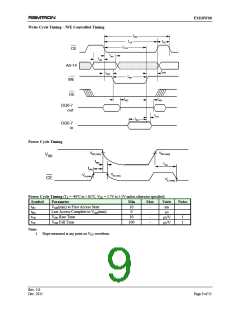
tWZ
tWX
tHZ
tWS
tWH
Notes
Write Enable Low to Output High Z
Write Enable High to Output Driven
Chip Enable to Output High-Z
Write Enable Setup
15
15
15
15
ns
ns
ns
ns
ns
1
1
1
2
2
10
10
0
0
0
0
Write Enable Hold
1
2
This parameter is periodically sampled and not 100% tested.
The relationship between /CE and /WE determines if a /CE- or /WE-controlled write occurs. There is no timing
specification associated with this relationship.
Data Retention
Symbol
TDR
Parameter
@ +85ºC
@ +80ºC
@ +75ºC
Min
10
19
Max
Units
Years
Years
Years
Notes
-
-
-
38
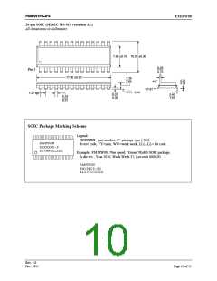
Rev. 2.0
Dec. 2011
Page 7 of 11

 RAMTRON [ RAMTRON INTERNATIONAL CORPORATION ]