in the appropriate bank and its corresponding SRAM cache
DRAM Read Hit
A DRAM read request is initiated by clocking /RE with W/R low
simultaneously to maintain coherency. The write address and data are
posted to the DRAM as soon as the column address is latched by
bringing /CAL low and the write data is latched by bringing /WE low
(both /CAL and /WE must be high when initiating the write cycle with
the falling edge of /RE). The write address and data can be latched
very quickly after the fall of /RE (tRAH + tASC for the column address
and tDS for the data). During a write burst sequence, the second write
data can be posted at time tRSW after /RE. Subsequent writes within a
page can occur with write cycle time tPC. With /G enabled and /WE
disabled, it is possible to perform cache read operations while the /RE
is activated in write hit mode. This allows read-modify-write, write-
verify, or random read-write sequences within the page with 12ns
cycle times (the first read cannot complete until after time tRAC2). At
the end of a write sequence (after /CAL and /WE are brought high and
tRE is satisfied), /RE can be brought high to precharge the memory. It
is possible to perform cache reads concurrently with precharge.
During write sequences, a write operation is not performed unless
both /CAL and /WE are low. As a result, the /CAL input can be used as
a byte write select in multi-chip systems. If /CAL is not clocked on a
write sequence, the memory will perform a /RE only refresh to the
selected row and data will remain unmodified.
and /F and /CAL high. The EDRAM will compare the new row
address to the last row read address latch for the bank specified by
row address A (LRR; an 9-bit latch loaded on each /RE active read
2, 9
cycle). If the row address matches the LRR, the requested data is
already in the SRAM cache and no DRAM memory reference is
initiated. The data specified by the column address is available at the
output pins at the greater of times tRAC1, tAC, tGQV, and tASC + tCLV.
Since no DRAM activity is initiated, /RE can be brought high after
time tRE1, and a shorter precharge time, tRP1, is required. It is
possible to access additional SRAM cache locations by providing
new column addresses to the multiplex address inputs. New data is
available at the output at time tASC + tCLV after each column address
change.
DRAM Read Miss
A DRAM read request is initiated by clocking /RE with W/R low
and /F. The EDRAM will compare the new row address to the LRR
address latch for the bank specified by row address bits A (LRR:
2, 9
9-bit row address latch for each internal DRAM bank which is
reloaded on each /RE active read miss cycle). If the row address
does not match the LRR, the requested data is not in SRAM cache
and a new row must be fetched from the DRAM. The EDRAM will
load the new row data into the SRAM cache and update the LRR
latch. The data at the specified column address is available at the
output pins at the greater of times tRAC, tAC, tGQV, and tASC + tCLV. It is
possible to bring /RE high after time tRE since the new row data is
safely latched into SRAM cache. This allows the EDRAM to
precharge the DRAM array while data is accessed from SRAM cache.
It is possible to access additional SRAM cache locations by
providing new column addresses to the multiplex address inputs.
New data is available at the output at time tASC + tCLV after each
column address change.
DRAM Write Miss
A DRAM write request is initiated by clocking /RE while W/R,
W/E, and /F are high. The EDRAM will compare the new row address
to the LRR address latch for the bank specified for row address bits A
2, 9
(LRR: a 9-bit row address latch for each internal DRAM bank which is
reloaded on each /RE active read miss cycle). If the row address does
not match any of the LRRs, the EDRAM will write data to the DRAM
page in the appropriate bank and the contents of the current cache is
not modified. The write address and data are posted to the DRAM as
soon as the column address is latched by bringing /CAL low and the
write data is latched by bringing /WE low (both /CAL and /WE must be
high when initiating the write cycle with the falling edge of /RE). The
write address and data can be latched very quickly after the fall of /RE
(tRAH + tASC for the column address and tDS for the data). During a
write burst sequence, the second write data can be posted at time tRSW
after /RE. Subsequent writes within a page can occur with write cycle
time tPC. During a write miss sequence, cache reads are inhibited and
the output buffers are disabled (independently of /G) until time tWRR
after /RE goes high. At the end of a write sequence (after /CAL and /WE
DRAM Write Hit
A DRAM write request is initiated by clocking /RE while W/R, W/E,
and /F are high. The EDRAM will compare the new row address to the
LRR address latch for the bank specified by row address bits A2, 9(LRR:
a 9-bit row address latch for each internal DRAM bank which is
reloaded on each /RE active read miss cycle). If the row address
matches the LRR, the EDRAM will write data to both the DRAM page
EDRAM Basic Operating Modes
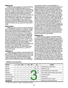
Function
/CAL /WE
A
Comment
No DRAM Reference, Data in Cache
DRAM Row to Cache
/F
H
H
H
H
L
/S
L
/RE
↓
W/R
L
0-10
Read Hit
H
H
H
H
X
H
X
L
X
X
H
H
X
H
X
H
Row = LRR
Read Miss
Row ≠ LRR
L
↓
L
Write Hit
Row = LRR
Write to DRAM and Cache, Reads Enabled
Write to DRAM, Cache Not Updated, Reads Disabled
Cache Reads Enabled
L
↓
H
Write Miss
Row ≠ LRR
L
↓
H
Internal Refresh
Low Power Standby
Unallowed Mode
X
X
X
X
X
H
H
H
↓
X
Standby Current
H
L
↓
X
X
H
H
Unallowed Mode (Except -L Option)
Standby Current, Internal Refresh Clock
X
Low Power Self
Refresh Option
X
H = High; L = Low; X = Don’t Care; ↓ = High-to-Low Transition; LRR = Last Row Read
2-97

 RAMTRON [ RAMTRON INTERNATIONAL CORPORATION ]