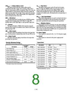
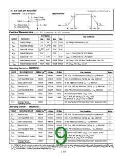
AC Test Load and Waveforms
V Timing Reference Point at V and V
IN
IL
IH
Load Circuit
5.0V (3.3V Option)
Input Waveforms
V
V
IH
IH
R1= 828Ω (5 Volt)
R1= 1178Ω (3.3 Volt)
Output
V
V
IL
IL
R2 = 295Ω (5 Volt)
R2 = 868Ω (3.3 Volt)
C L = 50pf
GND
≤5ns
≤5ns
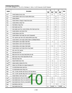
Electrical Characteristics TA = 0 - 70°C, (Commercial), -40 ~ 85°C (Industrial)
3.3V Option
Test Conditions
All Voltages Referenced to V
Symbol
Parameters
Max
Max
4.75V 5.25V
Min
Min
V
Supply Voltage
3.0
3.6
SS
CC
V +0.3V
CC
V
Input High Voltage
Input Low Voltage
Output High Level
Output Low Level
Input Leakage Current
2.0
2.4V
6.5V
IH
V -0.3V
SS
V
IL
0.8V
0.4V
-1.0V 0.8V
2.4V
V
2.4V
I
= - 5mA (-2mA For 3.3V Option)
OUT
OH
V
0.4V
I
= 4.2mA (2mA For 3.3V Option)
OL
OUT
I
I
-90µA 90µA -180µA 180µA
OV ≤ V ≤ 6.5V, All Other Pins Not Under Test = 0V
IN
i(L)
Output Leakage Current -90µA 90µA -180µA 180µA
OV V , OV V
5.5V
≤
OUT
≤
≤
IN
O(L)
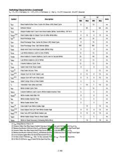
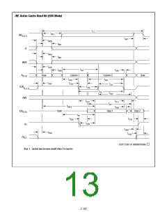
Operating Current — DM2M32SJ
33MHz Typ(1)
-15 Max
1440mA 1440mA /RE, /CAL, /G and Addresses Cycling: t = t Minimum
Symbol
Operating Current
Random Read
-12 Max
Test Condition
Notes
I
880mA
2, 3
CC1
C
C
I
Fast Page Mode Read
Static Column Read
Random Write
520mA
920mA
720mA
1200mA
840mA
16mA
920mA /CAL, /G and Addresses Cycling: t = t Minimum
2, 4
2, 4
2, 3
2, 4
PC PC
CC2
I
440mA
1080mA
400mA
16mA
720mA
1200mA
840mA
16mA
/G and Addresses Cycling: t = t Minimum
SC SC
CC3
I
/RE, /CAL, /WE and Addresses Cycling: t = t Minimum
C
C
CC4
I
Fast Page Mode Write
/CAL, /WE and Addresses Cycling: t = t Minimum
PC PC
CC5
I
Standby
All Control Inputs Stable
/S, /F, W/R, /WE and A
V
- 0.2V
≥
CC6
CC
at V -0.2V,
≥
I
0-10
Self-Refresh (-L Option)
1.6mA
1.6mA
1.6mA
CC
CC7
/RE and /CAL at
V
<
+ 0.2V, I/O Option
SS
I
1
Average Typical
Operating Current
240mA
—
—
See "Estimating EDRAM Operating Power" Application Note
CCT
Operating Current — DM2M36SJ
33MHz Typ(1)
990mA
-15 Max
Symbol
Operating Current
Random Read
-12 Max
Test Condition
Notes
I
2025mA 1620mA /RE, /CAL, /G and Addresses Cycling: t = t Minimum
2, 3
CC1
C
C
I
Fast Page Mode Read
Static Column Read
Random Write
585mA
1305mA 1035mA /CAL, /G and Addresses Cycling: t = t Minimum
2, 4
2, 4
2, 3
2, 4
PC PC
CC2
I
495mA
1215mA
450mA
18mA
990mA
810mA
/G and Addresses Cycling: t = t Minimum
SC SC
CC3
I
1710mA
/RE, /CAL, /WE and Addresses Cycling: t = t Minimum
1350mA
C
C
CC4
I
Fast Page Mode Write
1215mA 945mA
/CAL, /WE and Addresses Cycling: t = t Minimum
PC PC
CC5
I
Standby
18mA
1.8mA
18mA
1.8mA
All Control Inputs Stable
/S, /F, W/R, /WE and A
V
- 0.2V, Outputs Driven
≥
CC6
CC
at V -0.2V,
≥
I
0-10
Self-Refresh (-L Option)
1.8mA
CC
CC7
/RE and /CAL at
V
<
+0.2V, I/O Option
SS
I
1
Average Typical
Operating Current
270mA
—
—
See "Estimating EDRAM Operating Power" Application Note
CCT
(1) “33MHz Typ” refers to worst case I expected in a system operating with a 33MHz memory bus. See power applications note for further details. This parameter is not 100% tested
CC
(3) I is measured with a maximum of one address change while /RE = V .
or guaranteed. (2) I is dependent on cycle rates and is measured with CMOS levels and the outputs open.
CC
IL
CC
( 4) I is measured with a maximum of one address change while /CAL = V .
CC
IH
2-103

 RAMTRON [ RAMTRON INTERNATIONAL CORPORATION ]